This is part 2 of my future phone 2025 vision article, for part 1, check out the post here. This part details out the features that could be in Phone 2025!
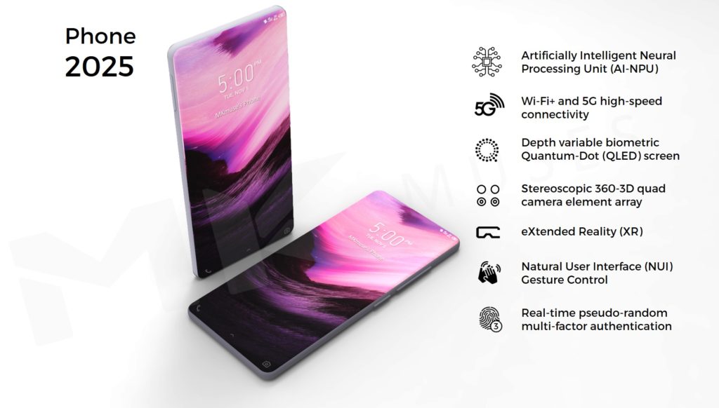
Neuromorphic processor with an “AI-core”
Existing smartphones have been demonstrated to digitize
documents, translate signs, drive a car, solve a Rubik’s cube, and the 2025 phone will become a
butler, providing information that you didn’t know you needed, giving answers
and solutions as you command it, learning your habits, nuances and behaviors to
essentially offset human weaknesses.
For that to happen, the processor needs to be powerful
– as powerful as a human brain, but without its caveats, such as forgetfulness.
The processor will be a multi-SoC (system on chip) and will have the standard
CPU-GPU cores, but with a Vision Processing Unit (VPU) and a neuromorphic core or Neural Processing Unit
(NPU). This CPU-GPU-VPU-NPU processor will pave the way for Artificial
intelligence (AI) of the future.
For the sake of simplicity, I call this neuromorphic
processor an Artificially Intelligent Neural Processing Unit (AI-NPU). With
machine-learning algorithms and neural-network (NN) circuitry, this AI-NPU core
will feature deep-learning capability and the smartphone will learn to
anticipate what I want to do next, my schedules, habits, desires and needs in a
more human-like manner than the semantic feedback we have today.
A neuromorphic core is a processor
modeled after the human brain, designed to process sensory data such as images and sound and
respond to changes in that data in ways not specifically programmed. A learning
and constantly evolving core computing architecture is tremendously efficient
as it finds new and better ways to process a task. It’s like learning how to
ride a bicycle. Despite the complexity of the activity, after a few tries, the
task becomes ingrained and effortless, and the brain now automatically
maintains balance and speed to keep a bicycle in motion.
With human-like anticipation and realism, you will not
be able to tell the difference between your phone and a person. By learning
texting habits, the phone will be able to respond to messages by itself, like
having a bot to reply to those tedious chats. The new processor will make Bixby,
Alexa, Siri and Cortana jealous.
The semiconductor industry has been pretty consistent
in its projected advancements, with major players investing billions of dollars in R&D, and I expect to see a powerful
CPU shrink down in size to fit my smartphone in 2025.
Computing Desktop environment
With all that processing power in a phone, do we really
need a laptop or tablet for everyday computing tasks? The future phone will
become your future laptop or desktop with a simple dock.
The idea is not new. Since 2012 Asus has had a product line, the PadFone, where its smartphone could be
docked into a tablet – increasing the screen real estate and battery life of
the phone.
This desktop functionality concept was recently updated
by Razer’s Linda, Microsoft’s Continuum and Samsung’s DeX. Linda turns a smartphone into a
trackpad that docks into a laptop body, whilst Dex is a dock for a phone which creates a familiar desktop
computing environment. This desktop PC feature will be mainstream in future
phones just by plugging a reversible USB Type-C port into the phone for both
graphics and power. Examples today include Continuum and DeX, which can run from the company’s flagship phones. You’d be surprised
how something so simple still isn’t intuitive enough today.
I envision that in 2025, we will all be carrying our PC
in our pocket, looking for USB-C ports to plug our phones into so we can
display our own instant-on PC at work, a friend’s home, or just about anywhere.
I’ll wake up, undock my phone from its wireless-charging cradle and, when I
reach work, I’ll just dock my phone into the cradle at my desk. There is would
be no need for a dedicated computer at work or at home. All files are stored on
various cloud services (Dropbox, Google Drive, Onedrive), while persistent
files are stored in the phone’s 16TB of storage.
A home, or in the office, projectors and screens receive
wireless display commands from the phone that are compatible with existing wireless display
standards such as
Apple’s AirPlay, Miracast, Intel Wireless Display (WiDi) and DLNA. As a
computing desktop, our 2025 phone will push or stream a desktop screen to any
TV, projector or screen that is compatible.
You’ll finally be free of lugging around a laptop. Just
think about that.
Connectivity
The phone will have the latest connectivity options
built into its communications chips.
5G-New Radio (5G-NR) is slated to replace 4G.
4G-LTE was introduced in 2009 and it took a few years for the infrastructure to
become mainstream. 5G is in its infancy now, and 900% improvement has been demonstrated by Qualcomm over existing 4G networks.
By 2021, we should see 5G become mainstream in mobile
devices and commonplace in the 2025 phone, with upgrades over existing
standards. The increased speed and
bandwidth that enables 5G is the use of a broader spectrum of frequencies and multiple antenna arrays. The standard also allows
device-to-device communication, allowing your phone to be the central hub or
base station controlling all your other IoT gadgets in the vicinity. Major
chipmakers Qualcomm, Intel and Huawei all announced their 5G
modems this year.
As for Wi-Fi connectivity, the standard that is known
as the IEEE 802.11ax, now referred to as Wi-Fi 6 that was just introduced
this year, will be mainstream in our Phone 2025.
The new standard feature – Multiple-input
multiple-output orthogonal frequency-division multiplexing (MIMO-OFDM) – allows
bandwidth speeds five times faster than today’s fastest 802.11ac networks. Also,
with CO-MIMO antenna arrays, users will experience even
faster connectivity when there are several base-stations or routers nearby, as
each data stream is broken up or provided by several routers. A very important
speed upgrade when streaming 4K-Mixed-Reality (4K-MR) data streams is aptly
shown in the Vimeo video in the next section.
With new bandwidth pipelines streaming directly to the
future phone, users will demand ever greater instant high-quality content and
information. Search, e-commerce and information avenues will grow ridiculously,
with instant online demand from consumers. It is one of the reasons Google is
paying a premium to have its search engine natively
installed on Apple devices. The revenue line between the future phone and
content/shopping services will blur and we could see major search engines and
retailers putting resources into developing their own phones such as the Google
Pixel 4 and Amazon’s foray into the
smartphone market.
The motivation is simple, the future phone is the de
facto portal to content, products, and services.
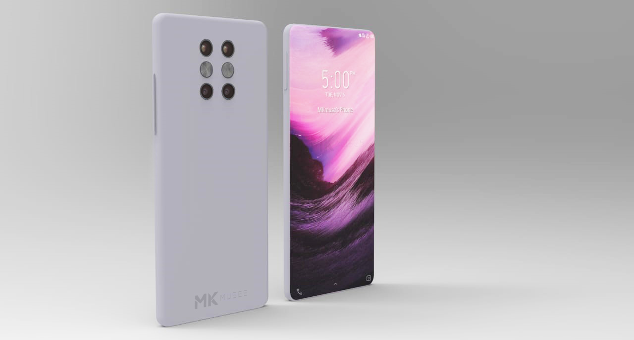
Screen
technology has come a very long way since the last decade of smartphones, with
pixel densities gradually increasing and pixel sizes slowly decreasing, with the
first high-density pixel displays
marketed by Apple, as a “retina-screen”, and Samsung’s Super AMOLED both
exceeding 200-pixels per inch (ppi) then, and today to 458ppi on the iPhone 11
and 401ppi on the Samsung S10.
Our
smartphones have captured all of our visual attention. Americans spend three to four hours a day
looking at their phones,
and about 11 hours a day looking at screens of any kind. Needless to say,
the screen is still the main interactive surface with the Phone 2025, only that the technologies used to
build the screen are going to be amazingly different. Today’s screens are
typically built on AMOLED, IPS-LCD or OLEDs, but upcoming technologies such as
a microLED (mLED) are in the works.
I think that QLEDs (quantum-dot) LEDs will become a
mature mobile screen technology capable of giving us the chromatic vibrance consumers
demand. Quantum-dot displays are not a new technology and are
staples of flagship television products today, with manufacturers touting the
advantages of QLEDs compared to OLED TVs. A nice comparison is described here. However, QLEDs are still nascent
and there is massive commercial push to advance this technology.
I’m just going to call it what it
is, the future phone will sport a QLED 4K ultra-resolution screen likely based
on electroluminescent quantum dots (ELQD) and… it will be transparent. Why do we need a transparent QLED
screen?
We can now hide the front cameras
and sensors behind the screen. Since the nano-pixels of the QLED screen are so
small, tiny holes or gaps can be created between the light-emitting pixels to
allow light through the screen. Looks like Oppo has already unveiled this cool feature!
No more notches or front-facing
sensors taking up precious screen area. Just one big gorgeous edge-to-edge QLED
screen.
Another cool feature of Phone 2025 is the use of smart
nano-optics to create a depth perception, allowing the screen to produce a 3D
in-depth effect, some sort of holographic screen viewing experience, this capability
is important when we use the phone in eXtended Reality (XR) applications.
This new screen is transparent to cameras and biometric sensors behind the screen and allows depth/dioptre correction so that the display adjusts according to the distance that your eyes are away from the screen. If the screen is close to the user’s eyes, it blurs or sharpens reciprocally avoiding the need for corrective optics in XR headsets.
So the trend of having multiple
cameras started out once again from Apple, with the introduction of the iPhone
X’s dual camera, allowing for different lens elements (wide or telephoto). Manufacturers
quickly caught onto the advantages of having more than one camera module and
soon we had triple (Huawei’s P20 Pro & the Apple iPhone 11 Pro),
quad (Samsung Galaxy A9)
and even five cameras (Nokia PureView 9).
The main difference between the cameras are the
different focal lengths. The shorter the focal length, the wider the angle of
view and vice versa. It’s almost like carrying a full set of lenses in your
pocket.
Ok so we’ve got some wide-angle shots and some nice
zoomed-in shots. So what? What can we do with our two eyeballs that our phone’s
camera array will allow us to do better?
It’s
simple physics. More cameras mean the phone can capture more light. Meaning impressive
low-light vision and photography, a feature available in Huawei’s P30,
Google’s Pixel 3
and Apple’s iPhone 11 Pro.
I’m talking about Night-Vision.
So,
the Phone 2025 will have an optically stabilized quad camera element array with
the following camera capabilities:
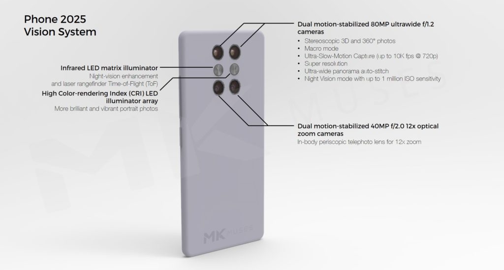
Telephoto Zoom In 2007, I thought a liquid-zoom lens would be a cool feature to allow for optical-zoom. After all, you still need actual physical distance to focus light from a distance to the sensor. Then Oppo and Huawei both offered phones with embedded lens elements in a periscopic manner within the camera body. That works too, let’s have two in the future phone.
Macro Mode (microscope) With up to 1cm focal distance from the ultra-wide, ultra-high-resolution main camera, loss of resolution to achieve macro-distances
Night Vision mode in real-time First, each sensor combines four pixels into one, and then we have light being captured on all four sensors simultaneously to create a true low-light camera, something popular low-light camcorders are known for. An infrared matrix illuminator beside the camera will help illuminate pitch-black conditions.
True-3D videos A quad camera setup will provide stereoscopic vision and depth-differentiated videos. Because there are now always at least two stereoscopic cameras capturing footage with distance information capture, Phone 2025 essentially becomes a 3D video camera capturing 3D volumetric videos and data. Capture 4K 120 frames per second (fps) 3D-video on this slick future phone.
Super Resolution photos Super Resolution is a technique that combines all the pixels from the different elements to form one ultra-large resolution photo. The technique differs slightly from night-vision mode where all the pixels are layered on top of one another to create a brighter image. Super Resolution photos combine each pixel side by side to make a larger image. There are commercial cameras using this technique – the Light L16 Camera from Light.co contains 16 camera modules – five 28mm ƒ/2.0, five x 70mm ƒ/2.0, and six 150mm ƒ/2.4 lenses giving a combined resolution of up to 52 million+ pixels! In fact LG has filed a patent for a 16-camera module phone. SIXTEEN.
You don’t need that many.
Ultra-Slow-Motion Capture Fast, sensitive cameras plus a crazy powerful processor equal ultra-slow-mo videos. Sony’s Xperia XZ3 can do 960fps at 1080p. I’d reckon Phone 2025 can do 4000fps at 1080p, no sweat. But the higher the fps, the smaller the resolution. Hey, you can’t have everything.
360° 3D videos Something I would like to see integrated into Phone 2025 is a 360° camera. How cool is that? Today’s 360° cameras, such as the Insta360 and GoPro Fusion, already produce jaw-dropping video features such as “over capture”. Because the camera is capturing 360 traditional frames can be captured from the spherical 360° video footage taken from a single camera point – giving the illusion of a panning camera with a moving subject, ‘bullet-time’ effect so on and so forth.
It’s like many cameras capturing the action all at once. This dream phone would be able to capture simultaneous video from the front and rear camera sensors. With four video streams, two from the front and two from the rear cameras, the AI-NPU stitches it all together.
XR eXtended Reality
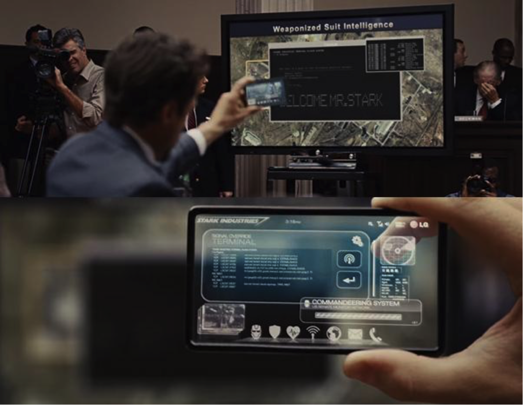
Phone 2025 has a powerful processor and powerful “eyes”
What else would be cool? Something like Tony Stark’s phone in the movie Iron Man 2. Rather, a mixed-reality with
AI-machine vision that will enable one to mark out or pull data spatially from the
environment.
Today, this is known as a technology-mediated
experience that combines virtual and real-world environments and realities,
often referred to as Augmented Reality (AR) or Mixed Reality (MR), where some
aspect of the real world can be seen, like Microsoft’s HoloLens; or Virtual Reality (VR) like the VIVE
system, where the
user sees a video feed instead of the actual environment.
The ‘X’ in eXtended is a placeholder for virtual
reality V(R), augmented reality A(R) or mixed reality M(R), and XR is can be
used to casually group technologies such as VR, AR and MR together. In a
nutshell, XR allows us to augment digital
objects or information on top of reality, or, conversely, see physical objects
as present in a digital scene. There have been many attempts such as the Ghost, and even this cool hyper-reality video concept done
by Keiichi Matsuda
and another concept by Unity.
Ok so what can we do with XR?
Simple stuff we can do today involves real-time
translation: Google’s Translate app translates multiple languages, Photomath solves any math problem you take a picture of and Google
maps helps you navigate in an urban environment.
When
app stores for the smartphone were introduced, they paved the way for an
industry of applications and businesses with promises of XR-enabled
technologies that would revolutionize the way we interact with our future
smartphones.
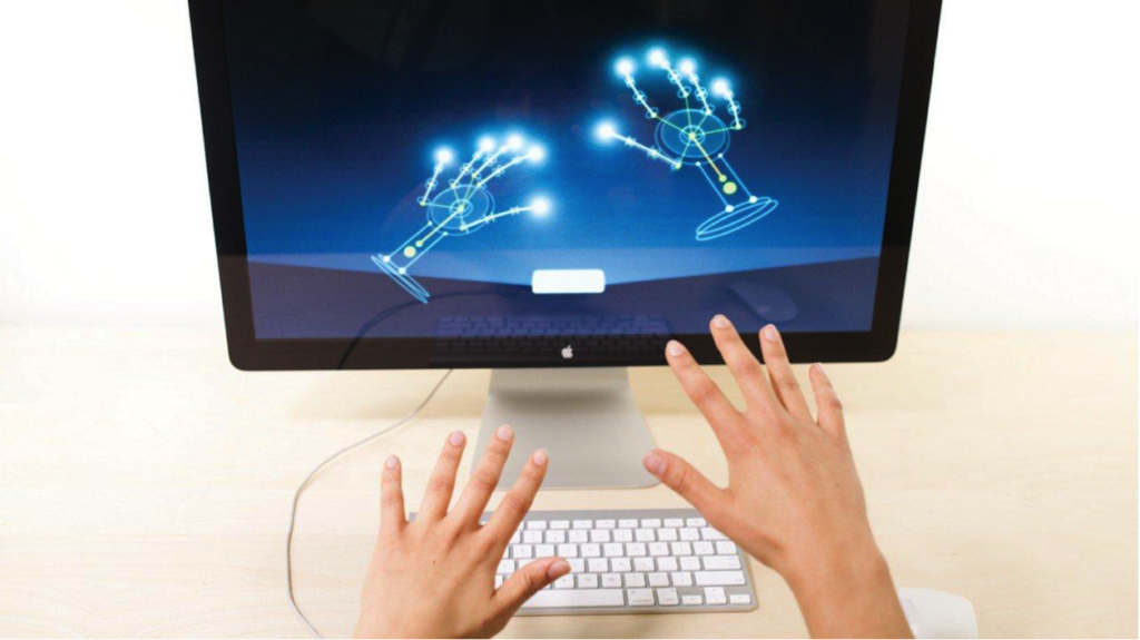
How are you
going to control your fancy MR headset? With XR and a computing desktop
environment enabled smartphone chances are, we could end up interacting with
what’s called a Natural User
Interface (NUI).
Despite the options available, the challenge has been miniaturization, the
sensor would have been placed underneath the QLED screen and could either be an
optical sensor or just plain old dual-cameras and machine-vision in action and
that’s not difficult to implement in a mobile device.
The truth is, having an NUI reduces the learning curve of new
applications and is critical in XR applications, where the ability to emulate
holding or interacting with a virtual object will greatly increase usability of
our future phone on many productivity fronts.
Fancy a future with people waving and gesticulating at their phones, that’s
body language indeed.
Hybrid Biometrics and Security
The Phone 2025 represents your
entire digital life, and with that, we will need upgraded security. Since the
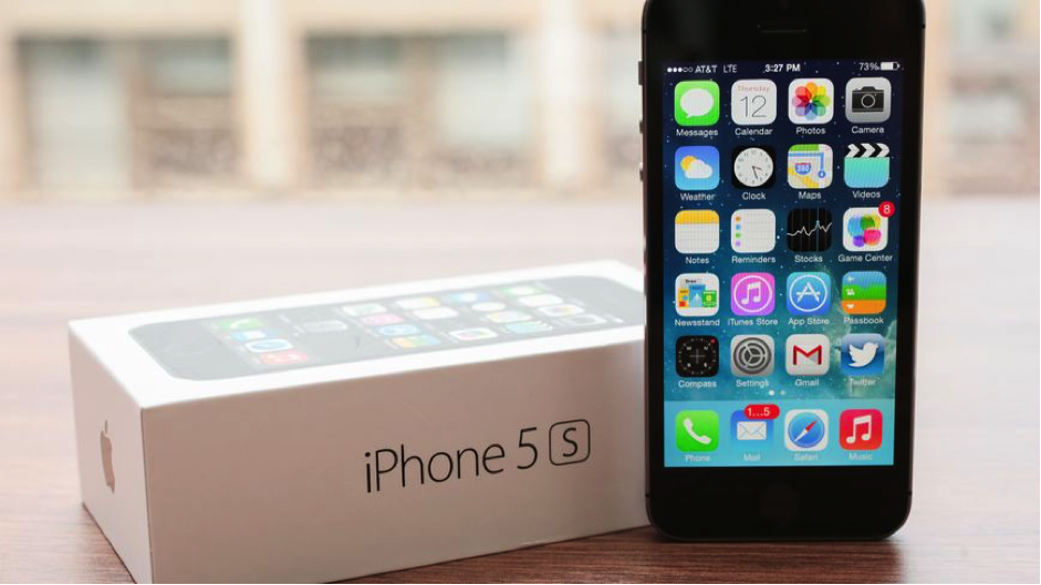
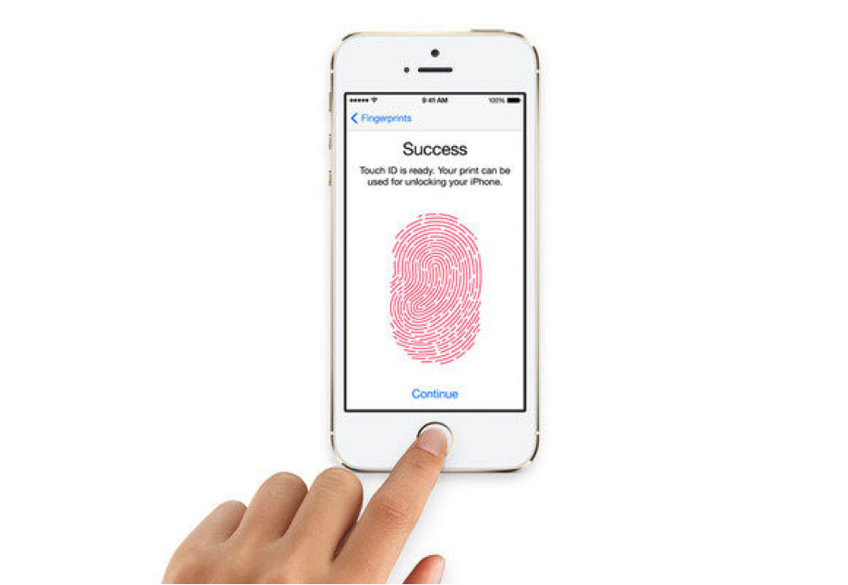
first fingerprint sensor on the iPhone5S, there have been some exciting
developments in this aspect, such as facial
and iris-recognition on 2017 flagship smartphones such as the iPhone X and
Samsung Galaxy S9.
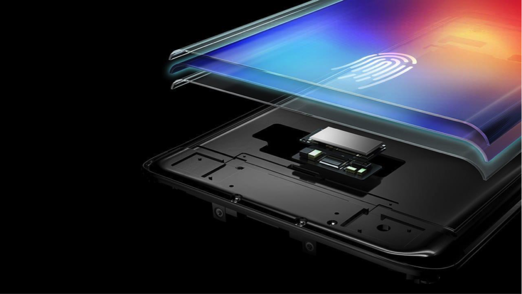
But how do designers pursue better
screen-to-bezel ratios without sacrificing fingerprint sensor footprints? This year,
several manufacturers introduced a dozen phone models with under-display
fingerprint sensors, such as the Vivo X21, Oppo R17, Huawei
Mate P30 Pro, Samsung Galaxy S10, Honor 20 Pro and OnePlus 6T provided by
manufacturers from Qualcomm, General Interface Solution (GIS),
O-film Tech,
Fingerprints
and Goodix.
However, we’ve seen that
fingerprint and facial recognition security methods can be spoofed or defeated.
How can we create a more secure device without sacrificing screen real estate? I dub the
next generation of biometrics in the future phone as Multi-factor
authentication (MFA), using no less than five biometric
factors at pseudo-random intervals. Full-display fingerprint scanner,
facial-recognition, capacitive
fingerprinting, blood-flow thermography are technologies that come to mind.
The entire QLED screen would
authenticate each finger-press as we tap anywhere on the screen, something Apple
patented in April 2019, and I envision the future phone to have thermogram
sensors to capture heat information as you use the device. 3D face printouts or
fingerprint hacks won’t work anymore, as the person using the phone must be a
live human being.
Currently, the world’s
smallest thermal camera is the Lepton from FLIR, which is available here
and here,
but at $350, it’s an expensive component to put into a phone. This is where a
lower-cost component such as Panasonic’s thermo-graphic matrix sensor,
known as the GRID-eye AMG8833, could be used.
The future phone will have at least three biometrics, in-screen fingerprint authenticator
checking every time you type on the screen, and a thermal-augmented facial
recognition scan. This MFA approach gives confidence that only the owner
can access his very expensive, high-tech piece of gear.
Imagine using your
phone to unlock your work monitor. There won’t be nosy co-workers trying to
guess your password or spoof your fingerprint reader. There’s nothing to break into
if the device isn’t even there.
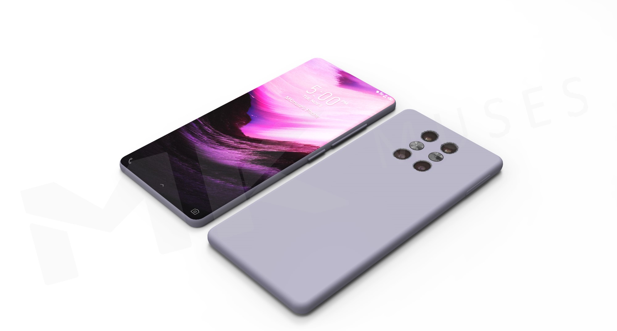
Phone 2025 Vision
Looks like I’m going
to wait out the next few phone releases till Phone 2025 is released!
Figure 1. What would we see in the next generation of smartphones? Check out Part 2 to see what I think!
It has been an interesting year
with half a dozen flagship smartphones released within months of each other by
major manufacturers. I thought the fall 2019 series of iPhones was an interesting sign of things
to come and historically speaking Apple’s smartphones have been a benchmark
many strive to achieve. The topic of smartphones can dominate a dinner
discussion, with naysayers and pundits in supportive and dismissive stances on
the features of each new model.
Modern mobile phones have become
complex handheld computers that are expected to perform myriad workhorse and
entertainment functions. To meet the insatiable global consumer demand for the
latest smartphone, new flagship models are released in mere months and each new
smartphone is expected to dazzle consumers with new
differentiating and defining features.
The history of smartphones
changing our lives has since spanned decades and smartphones have since come a
long way. In 2013, I praised the iPhone 5S, and in the last few months major
manufacturers like Apple, Samsung and Huawei have been releasing new flagships
vying for a chunk of the $355-billion pie.
What’s all the fuss about?
The mobile phone race has come a
long way since the first iPhone disrupted the market in 2007 with its iconic
keyboard-less capacitive touchscreen that has largely remained unchanged and
revolutionized future smartphone designs.
Today the industry has become
extremely complex. Manufacturers are scrambling to differentiate themselves
with the smallest of features that could sway consumers to purchase their model
over a rival’s.
There is a plentiful list of
acquisitions of smaller technology companies by major manufacturers such as Apple and Samsung to create a significant
differentiator in their handsets. Individual components that defined a feature
in a handset could have been a purchase of an entire company’s product
portfolio by one of the larger smartphone manufacturers – for instance the purchase of AuthenTec for $356M in 2012 enabled Apple to lead the
market the following year with fingerprint biometrics in the iPhone 5S – a
major leap forward in phone security then.
Now, there is hardly a smartphone
without biometric security, immensely improving user experiences. With the
iPhone X, Apple once again rekindled the spotlight on the decades-old technology of facial
recognition –
which was available since 2012 on phones such as the HTC One X. The difference
is that Apple has vastly improved the feature with a “dot-projector” that
allows the facial recognition camera to work in low-light conditions and
greatly boosts resistance to spoofing attempts that plagued the older generation
of phones with that feature.
Hits and Misses
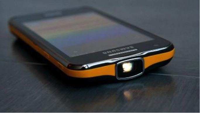
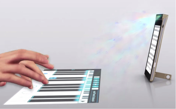
Over the years, there have been
some hits and misses. One example is an attempt by manufacturers to integrate micro DLP projectors to expand screen real estate by
projecting media and content onto an external surface such as Samsung’s Galaxy Beam and Lenovo’s Smartcast, which received a
lukewarm reception.
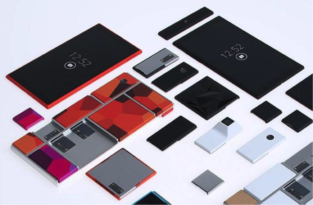
Other
misses were the much hyped “modular-phone” approach such as Google’s Project Ara and Motorola’s MotoZ (which is still available). The idea was simple –
users could customize their phone as they liked it – need a bigger battery? Use
a bigger battery module. Need more memory? Swap out a module with one of a
larger memory, and as better components were introduced to the market, users
could sequentially upgrade older components with newer modules and not have to
replace their entire phone. The concept was desirable on paper, but Google’s
Ara project never entered mass production and I don’t know anyone using a MotoZ
phone.
Then we have the first foldable smartphone with a flexible screen, the Samsung Galaxy Fold. The ambitious eye-watering $2,000 device got people excited with the idea that you could expand your phone to provide larger screen real estate, however it was possibly rushed to production resulting in a massive media disaster where many reviewers and users’ devices failed just days into use.
Trends Today
In 2018, 1.56 billion smartphones were sold worldwide and this trend is fueled by the
ravenous demand of consumers clamoring for more features and capabilities from
their handsets.
Mobile displays have resolutions exceeding what the
human eye can discern and their touchscreens have sensitivities greater than
our skin. These components are often very difficult to produce and competing
companies are forced into partnerships for parts sophisticated or too expensive
to produce for one smartphone model – for instance, Apple acquires its memory chips
and OLED screens from its rival Samsung for use in its iPhone X. It’s a peculiar relationship,
where the bulk of Samsung’s revenue comes from selling its best parts to its
competitor. These are used in Apple’s flagship phone, which outsells Samsung’s
own flagship phone, but when the iPhone X succeeds, so does Samsung!
Major players now use one another’s Intellectual
Property (IP) – a report breakdown of the iPhone X reveals that most
of its components are manufactured by other semiconductor companies. This
complex labyrinth of manufacturing logistics has spawned a global behemoth of
Original Equipment Manufacturers (OEMs), where companies produce parts that are
then resold or repackaged by another manufacturer.
The line blurs here, where now manufacturers have the
option of selecting parts of similar specifications and capabilities produced
for one brand for their own and hardware differentiation becomes
more difficult
moving forward, when every new flagship smartphone has very similar
specifications as its rival. Fast processor? Check. High-definition screen?
Check. Low-light zoom camera? Check. Waterproofing? Check.
This level of component inter-reliability is unprecedented,
with YouTuber Scotty Allen building a working Android phone and iPhone using back-alley components in Shenzhen, China.
Besides hardware features, software and user-experience
environment of the operating system becomes a glaring differentiator. Various
manufacturers add their own flavors based on their corporate strengths, such as
Google’s “unlimited” storage, where it provides its own cloud storage feature
(Google Drive) on its Pixel series – a seamless experience emulating a phone that doesn’t
have a storage capacity limitation. Other manufacturers have introduced their
own OS features such as Apple’s Siri and Samsung’s Bixby personal assistants, into their phones.
When it comes to battery life, as
there is a mismatch in technological advancement between chips and batteries,
it is more difficult to pack more energy into the same volume than transistors.
As processors get more capable and powerful, phone makers are compensating for
this incongruity by decreasing the size of the electronics to allow more space
and volume for batteries. As a result, phone designs have largely plateaued
into the same design across the market. A flat piece of metal and glass.
Unfortunately, when it comes to
hardware – there are only so many transistors one can cram into a processor or
sensor element. Semiconductor companies are packing more features and functions into their
chips using
increasingly sophisticated and expensive manufacturing methods that only the
big boys can afford.
It’s like watching a marathon
where best runners are neck and neck and no one can discern a clear winner,
whilst the rest of the competition has fallen far behind or dropped out.
Vision then and now
January 9th, 2007 was the day the world changed. Apple co-founder Steve Job presented the iPhone, which revolutionized the smartphone from a clunky keypad device to a desirable, sleek capacitive touch-screen communicator. That titular event rocked the mobile phone and computing industry and reinvented the meaning of a “mobile phone”.
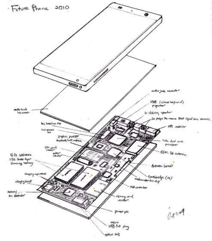
I remember the showcase vividly, enamored with how
technology leapt overnight. I realized we were in for a very different future
and sketched what I thought would be the phone of 2010.
Inspired by the first iPhone and the possibilities it
would bring and with existing advancements in 2007, I envisioned the following
features:
A liquid-zoom
lens that allowed actual telephoto-zoom capability into
the existing camera without physically moving a lens assembly.
16Gb of
memory (note that 2007-era phones had memory in the hundreds of megabytes).
USB3.0
charging port for high-speed data transfer and power charging and a large
4000mAh lithium-polymer battery to power this beefy device.
Wow. The future was something
to look forward indeed.
What has happened since?
Then 2010 came and the world
got Apple
iPhone 4 and Google’s
Nexus One. Both didn’t quite achieve my vision. The iPhone 4
had only 512Mb of DRAM memory and other flagships of the era had up to 1Gb of
on-board memory, a tad short of my envisioned 16Gb.
However, Samsung supplanted
that limitation with an external microSD card slot which allowed users to add
aftermarket memory of up to 32Gb in 2010. Moreover, those devices also
introduced features such as a high-resolution “retina
display”, video-chat and a gyroscope sensor to complement the
accelerometer. The addition of a high-resolution screen, a more powerful
processor and more sensors enabled a new generation of mobile games that were
controlled by the physical pan and tilt actions of the user.
A mark of exciting times.
Today,
there is no shortage of projections of “the future smartphone” with jazzy ideas
such as a foldable or bendable phone and fully transparent screens constantly
being featured by concept artists.
Unfortunately, whilst imaginative, there is a major
difference between an artistic concept and a manufacturable design, a fine
balance that Apple has been very successful in marrying. It is easy to envision
a bendable phone by introducing existing foldable batteries or flexible
electronics. However, unusual prototype or concept designs are notoriously
challenging to scale up to a mass production that meets consumer demand, or
very expensive to manufacture due to the low yield rate of a novel ingredient.
One missing component could require a complete redesign or an elimination of
that feature altogether.
An example would be a bendable phone, demonstrated in November 2018 by
Samsung and Royole. It’s arguable that whilst all components required to make a flexible
smartphone exist, there are a few problems – yield, availability and cost.
Flexible electronics do not yet have the component density of more established
rigid printed circuit boards (PCBs). There are fewer suppliers in the industry,
which means a higher cost and a lower yield to achieve the same performance of
rigid PCB counterparts. What about failure rates?
Samsung’s folding phone was a massive disaster, as no one wants a flexible
screen that fails after several hundred “folds” – a rigid screen is still more
reliable. Likewise, the same goes for a flexible battery, which does not have
the same energy density as the traditional lithium-ion battery pack, which has
an abundance of suppliers. These reasons are why I don’t think flexible phones
will become mainstream soon.
With these considerations and the current market inclinations, a future phone must be feasible, manufacturable and practical. With the highly random and unpredictable rapid advancement of technology amalgamated with the complexities of global manufacturing logistics and market economics, I’ve decided to envision a phone six years into the future. I present my Phone2025 concept, see my article on Part 2 of this segment!
“We are such stuff as dreams are made on, and our little life is rounded with a sleep.”
William Shakespeare, The Tempest
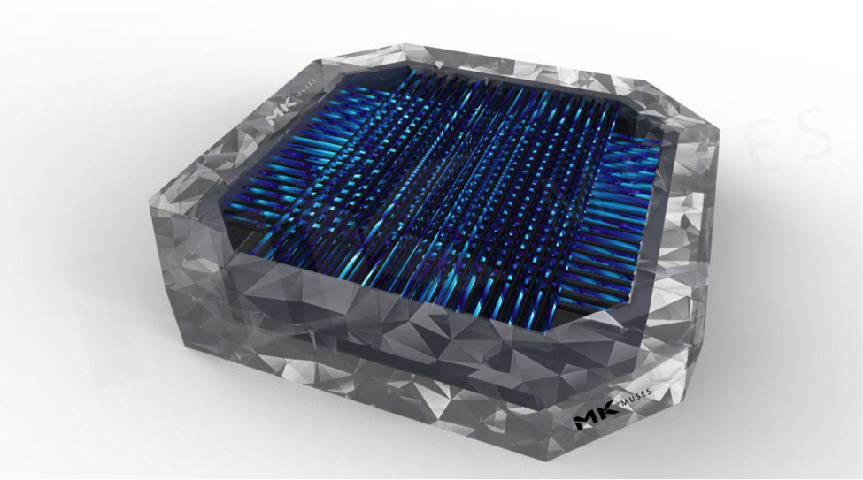
I present to you the Ontomorphic Quantum Processor – a beauty that came to me in a dream.
Sometime in the future
Imagine a scene out of the 2004 science-fiction action film I, Robot. Four men skilled in combat, myself included, were battling a humanoid robot in a tiny, claustrophobic room. We had trouble subduing it. The robot was nearly as quick as us – but it seemed invulnerable, with a tough composite alloy body. It fought in a windmill style, swinging its arms- metal arms that could cause serious damage to flesh and bone – in circles while rushing at us. There were no weaknesses we could exploit. It did not register pain and attacking it was like striking a lamp post.
The robot was state-of-the-art – more advanced than anything I’ve encountered in my dreams. It could process multiple assailants via its visual feed and anticipate attack vectors before we made our moves, compensating for its slower artificial muscle actuators.
I postulated that its processor is unlike anything humans have constructed. It likely created a real-time 3D response map and simulated every possible scenario and angle of attack from aggressors, while learning and analyzing fight patterns – think Ironman’s AI analyzing Captain America’s movements and countering them (in the Marvel Universe). Only our numerical superiority and teamwork finally brought down this robotic destroyer.
We removed the robot’s chest plate and, through a maze of wiring, found a cryogenic containment system. Why would a robot need a cryogenic system? One of my companions vented liquid helium from the vacutainer, nearly cold-burning his finger in the process. He released the inner pressure seal and that was when we witnessed this most advanced processor.
I consider myself relatively knowledgeable in the field of technology and we had a tech-wizard on the team who could lingo-speak with Tony Stark any day. The technology in front of us was generations ahead of anything we had faced and, given the paraphernalia required to run the processor, it became obvious what we had on our hands.
How a brain works
Our brains comprise neurons connected by dendritic synapses. Signals are first created from a neuron, known as an action potential, which is an electric signal created from chemical charge carriers known as ions. This electrochemical charge is then transferred via ions and neurotransmitters from one neuron to another. More details on the process are described here.
Computer processors work similarly. Almost every processor in use today is based on the manipulation of electrons – hence the term “electronics”. All information technology we have today follows the basic principle of sending electrons where we want them to go.
Batteries store electrons, transistors funnel and direct electrons, LEDs convert electrons to photons and, on a larger scale, integrated circuits are a bunch of transistors and switches turning on and off depending on how or where we want the electrons to go to.
Our brains process and store information via electrical signals, very similar to how computers do it. The only difference is we use neurons and computer processors, transistors. The problem with today’s processors is that you can cram only so many transistors into a piece of silicon.
Eventually, traditional transistor-based processors encounter heat and electron-leakage problems.
The future needs a futuristic processor.
Robotic brains in science-fiction
Science-fiction abounds with the fantastic imagination
of writers. The droids in I, Robot and the Star Wars film franchise are built
with “positronic
brains“, while the killer robots in the Terminator film franchise use
“neural net
CPUs“.
Since a positron or antielectron is the antiparticle or
the antimatter counterpart of the electron, I don’t think it’s implausible to
have a positronic processor as the manipulation of positrons could yield
superior processing power. Positrons are subatomic particles that have the same
mass as an electron, but a positive instead of a negative charge. When these
two particles encounter each other, they annihilate and produce two or three
gamma-ray photons, (high-energy light) in an event referred to as electron-positron
annihilation.
I’ve yet to see scientific evidence of how a positron manipulation is possible today and the most advanced scientific research into positrons are the creation and study of positrons. So, a positronic brain is still in the realm of science-fiction.
I’ve yet to see scientific evidence of how a positron
manipulation is possible today and the most advanced scientific research into
positrons are the creation and study of positrons. So, a positronic brain is
still in the realm of science-fiction.
Now, the neural net CPU in the Terminator franchise is
described to be based on quantum effect chips. Quantum computers
are no longer the stuff of science-fiction and are even commercially available
from Google and IBM.
Today’s quantum computer systems are in their
infancy and fraught with engineering challenges. They are almost comparable
to the first integrated circuit released in 1958. Over the last
six decades, the first integrated circuit has now become a supercomputing
device that fits in our palm – what we now know as a smartphone. Imagine going
back in time and showing someone from the 1960s the capabilities of your
smartphone. That piece of glass and metal in your hands would be considered
magic. The technology required to create a smartphone would have been
unfathomable then.
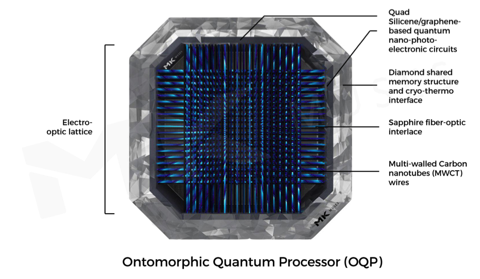
Ontomorphic quantum processor
Some 40 years into the future, the Ontomorphic Quantum Processor, which we dug out of the robot, is a self-learning quantum processor that does not need to be chilled to absolute zero to maintain quantum states. It is based on known science but is still beyond the capabilities of technology now.
The processor’s four interior walls contain four silicene/graphene-based quantum nano-electronic circuit boards. The circuits are then connected via what I call the electro-optic lattice. The lattice structure comprises optical and electrical conducting strings. The optical conductors transmit information photons of light via optical fibers made from yttrium aluminum garnet or sapphire crystals. The electrical wires are made from multi-wall carbon nanotubes that are superconducting in the cryogenic socket.
Four quantum circuits are enclosed by a large quantum memory crystal based on a diamond. This diamond-based quantum memory stores quantum information that is transmitted across the lattice via photons. If you compare it with today’s conventional processors, you could call this a quad-core CPU with shared memory, something already present in graphic processing units.
The lattice acts like a neural network, shoving light-signals where they need to go at near-light speed, and changes depending on the information being processed, which brings about its “learning capabilities” or the ontomorphic portion of this processor.
Wait… what?
Ontomorphic?
The word ontomorphic does not exist, but ontogeny refers to the inception and lifelong development of an organism physically and psychologically to its eventual maturity and subsequent senescence. I use this word because our human learning capabilities come from our interaction with our environment and experiences throughout our lives.
When one learns to perform a task, like ride a bicycle, do a cartwheel or master a new language, one is often awkward, clumsy and inefficient. But over time and practice, the brain forms new synaptic connections to streamline the knowledge.
One gets better, more efficient. That is the formation of new neural pathways in the brain, but the total number of neurons remains relatively the same.
This is the same for the Ontomorphic Quantum Processor. The number of quantum gates is limited by the initial design and construction of the processor, but the electrooptic lattice allows signals to be routed more efficiently over time. A simple example could be: “How can we arrive at 100 from 0?”
A child could start with 1 + 1 + 1 + 1 + 1… till he reaches 100. For this to happen, the child needs to understand the concept of numbers and the arithmetic function of addition. He would eventually arrive at the number 100. A triple-digit constant. Great!
Could this be done more effectively? A child introduced to the multiplication function could attempt a more efficient approach: 10 x 10 = 100. Even better. But now, the child needs to commit to memory what multiplication does and the tables associated with it.
All this assumes that no errors occur in the process, which is almost impossible. Which is where I come to the morphic capabilities of the
Ontomorphic Quantum Processor.
Learning and evolving from error
What is often referred to today as evolutionary or mutation computation is essentially a computer attempting a trial-and-error process to determine the most efficient and optimal solution. There will come a point where memorizing the entire multiplication tables will take too much memory to be viable or useful to the individual. What’s 5424 x 2413?
Yes, one could learn novel arithmetic to compute that mentally, but most adults will reach for a calculator. The process is comparable to determining that there’s a shortcut through an alley on your way home or discovering that a button on the photocopying machine scans a two-page document in half the time.
Evolution computation has been used to design more efficient antennas [12] and chairs, often exceeding what humans can envision manually. The ontomorphic capabilities of the Ontomorphic Quantum Processor come from the new junctions and spin-spin interactions from the electrooptical lattice, known today as neural networks [13], but much more advanced and far faster at near-lightspeed interaction.
This processor learns and becomes better at what it’s instructed to do.
Quantum computer
The primary principle of the Ontomorphic Quantum Processor is quantum logic [1], using quantum-mechanical superposition and/or entanglement to perform computation functions. Quantum computers are vastly different from traditional computers in that they use quantum logic gates and qubits and have the potential to compute complete equations hundreds of millions of times better than a traditional computer. In that perspective, today’s most advanced transistor-based processors would look like an abacus beside a quantum computer system.
Silicene/graphene nanoelectronic board
Quantum logic gates are delicate structures and
traditional printed circuit boards aren’t going to cut it. So silicene/graphene-based
boards are required [2] as a foundation for the nano-electronic circuits that
contain billions of quantum gates [3]. Silicene is an allotrope of
silicon, much like graphene
is an allotrope of carbon. Both have hexagonal honeycomb structures and exhibit
remarkable properties of electrical conductivity and functionalization Silicene
would provide the base for traditional transistor construction with its band-gap tunability
and stronger spin–orbit coupling which is important to maintain the Quantum spin Hall
effect. It’s as small as it gets – atomic-level transistors.
Graphene will be utilized as the circuit foundation,
for it is better at conducting electricity than copper, which makes it ideal
for ultra-fast circuits [4]. Moreover, graphene’s photovoltaic
effect has been shown to conduct electricity after absorbing light [5].
These two incredible properties of graphene mean optoelectrical signals can be
transferred from quantum gate to quantum gate at ultra-fast near-lightspeeds
[6].
The silicene/graphene nanoelectronic board will contain all the quantum gates and convert the signals and information from light to electricity and vice versa.
Quantum memory diamonds
As you can imagine, you probably can’t use traditional memory to store quantum information. Diamonds being used as quantum memory is a recent development [7-11]. Normally, a diamond is composed of only carbon atoms in a tetrahedral structure. Introducing a nitrogen atom into the structure instead of carbon and specific sites leaves a hole or vacancy in the crystal lattice. The nitrogen atom and the empty site can accept different quantum states and are used to store a quantum bit of information [11].
Diamond is an ideal material for quantum memory as the crystalline structure achieves strong coupling between phonons and vacancy spins which can be stored or read from as pulses of light, known as phonon-mediated quantum photonics [7, 8]. The probable reason why the diamond is arranged in such a way is to allow for shared-memory and faster access to memory from one nanoelectronic circuit board to another. Plus, diamond is an excellent heat conductor because of the strong covalent bonding and low photon scattering. Thermal conductivity of natural diamond is measured to be about 2200W/(m.K), five times more than silver, the most thermally conductive metal. This allows the whole processor to be effectively cooled to just above absolute zero to reduce quantum errors.
Year 2060
Computers have come a long way since 1960 and will continue to go further. Historically, there is an incredible breakthrough every century with major advancements in technology, from the bronze and iron ages to modern industrial, atomic and space ages.
Today, we are at the forefront of the information age
that is seeing no sign of stagnating, and systems are already incredibly
impressive. Isaac Asimov’s robot science-fiction novels have captured the
imaginations of many and many of his stories have become fact in recent years.
2060 will mark one century of computing progress and possibly the quantum age of mankind. Hopefully, I will live long enough to see it.
The performance of the Ontomorphic Quantum Processor will be unlike anything we can imagine today. It would perform more accurately and incredibly faster than any human can. That’s gonna rattle some cages.
Imagine seeing one firsthand. Now that will be exciting.
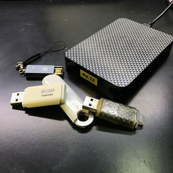
I’ve had my trusty 2TB Western Digital Passport for a while now, and a couple of thumbdrives of varying capacities lying around and as file sizes get bigger, instead of “how much capacity”, the question is now “how fast can I read/write my stuff?”
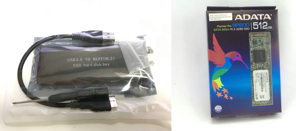
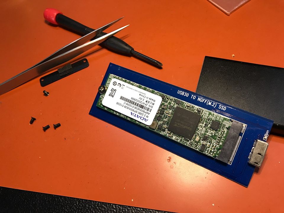
Transferring a 40Gb ISO file took forever, and I thought it was high time to upgrade. One of the biggest improvements in computing in the last decade was the growth of flash storage (storing data on chips instead of magnetic discs). Think about how much boot up and loading time SSDs have saved you. Speed aside, SSDs also have a size advantage. Today, it is possible to cram as much as 2TB of storage onto an M.2 drive the size and weight of a stick of chewing gum. Since all my PCs are on SSDs now it’s time to move away from hard drives. Up to 256Gb thumb drives exist now and Hardwarezone reviewed a couple of external SSD-based storage gadgets here. If you need more storage, there’s always Kingston’s new DataTraveler Ultimate Generation GT in 1 and 2 TB capacities. Kingston’s previous largest flash drive, the 1 TB DataTraveler HyperX Predator, is currently selling for over US$1,400 on Amazon as of July 2017. Yea. A thousand dollars for a thumb drive, oh well bragging rights are never cheap. I didn’t really need to carry 2Tb around all the time, and one grand is too much to stomach for a flash drive, so I went and assembled my own SSD-based thumb drive from an M.2 mSATA SSD. I got the M.2 to SSD converter enclosure here. There are other sellers that sell this item, however, it lacks a model number and thus you must search for it with generic search terms such as “NGFF USB 3.0”. You can pick one of these up for around $10 US. My SSD is a standard desktop grade M.2 by Adata SP900 2280 SATA in 512GB, based on synchronous MLC NAND flash and LSI SF-2281 controller, which I got for about $300.
Assembly
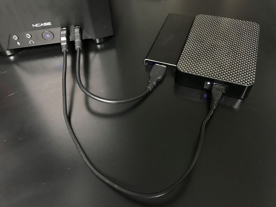
Pitting them head-on, both plugged into the USB3.0 port of my PC.
Performance benchmarking
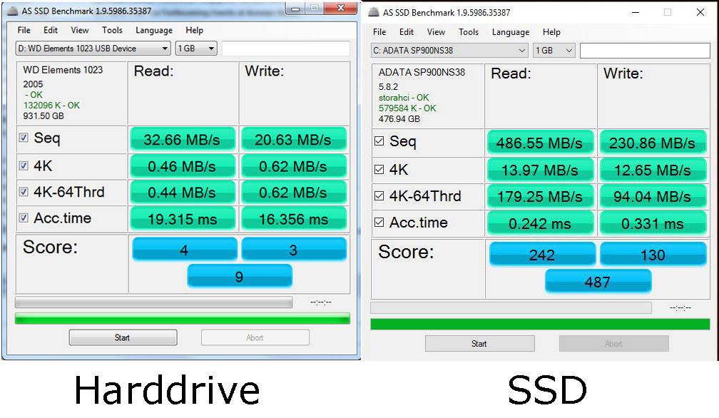
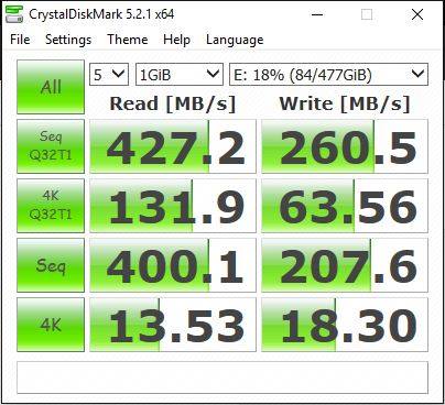
As expected, on an OS with UASP support, in this case Windows 10, we can connect in UASP mode. I was getting 427 – 486MB/s read and topping out at 230 – 260MB/s write speeds on the SSD across two benchmarking utilities, both more than ten times faster than the hard drive.
Real-world file transfer
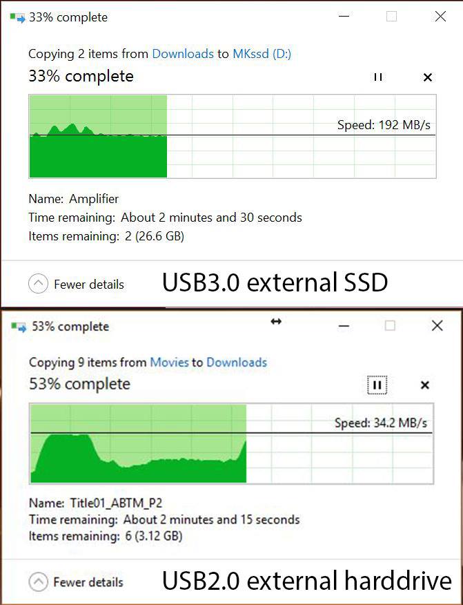
A simple un-optimized transfer with individual file sizes exceeding 4Gb saw an average speed of 192MB/s, nicely transferring 26.6Gb of data is 180 seconds, or about 3 minutes, reasonable with a bus write speed of 260Mb/s, the same transfer would have taken 1,016 seconds or 17 minutes on the harddrive!
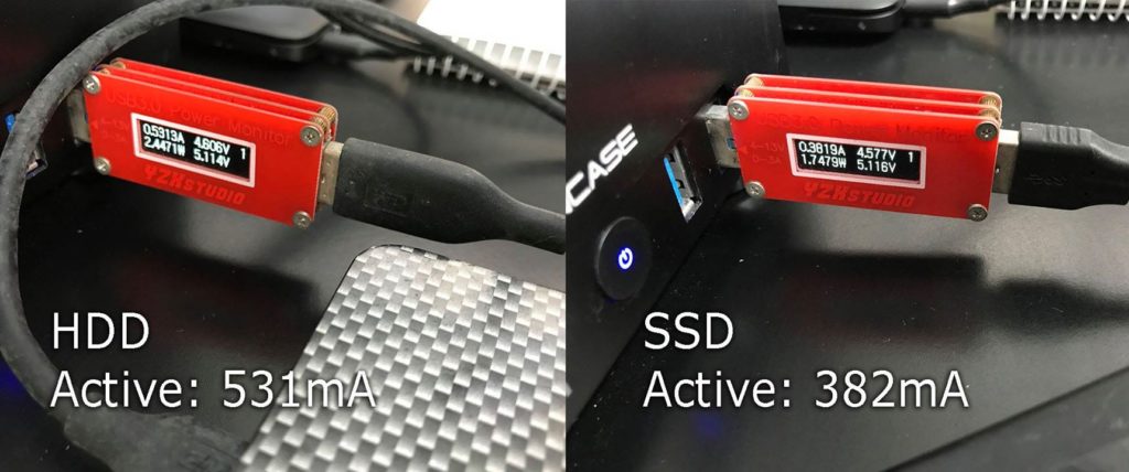
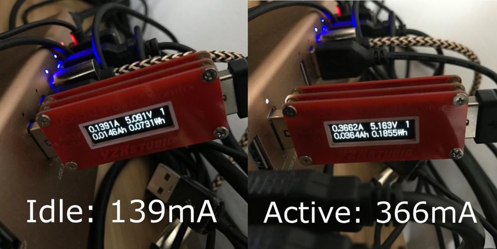
Power consumption
Power consumption is always a concern when you’re mobile, in this case my SSD consumes about 30% less power when active than my hard drive and idles at 139mA on average when there is no activity, significant when you’re on the road running off battery power.
The SSD consumes between 0.14A and 0.36A when idle and active (read/write).
Teardown
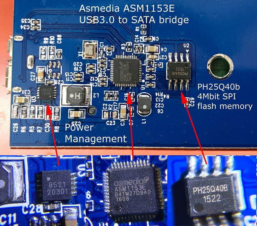
For geeks, the controller is based on the ASM1153E USB 3.0 to SATA III controller chipset from AS Media, the SOIC-8 PH25Q40B chip beside it is a SPI 4Mbit flash memory, which is likely used to store device ID reported to the host device as well as specific addresses of programming. Findchips and Octopart yielded nil results, but looking at the pin-outs and the footprint of the chip, it could be a clone of a similar 4MBit SPI 512KB x 8 NOR flash memory by Winbond with the part number “W25Q40B”
Verdict
Conclusion: All in all, I’m pretty satisfied with the results and hopefully it’ll last me for the next half a decade as my previous storage devices have reliably done so!
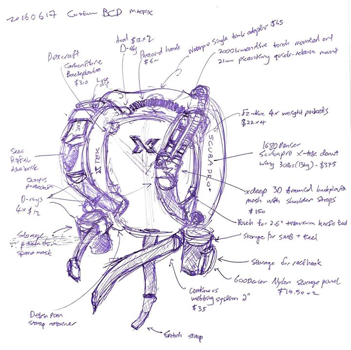
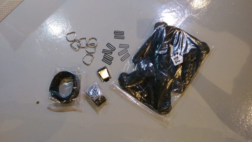
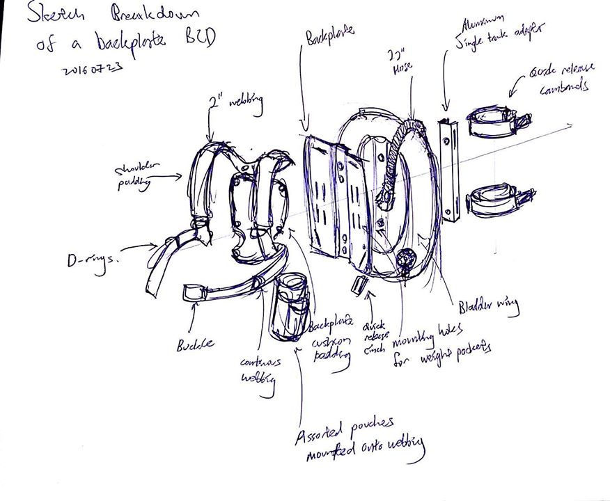
Hi all, several divers have asked me about my current buoyancy control device (BCD) configuration and I think it’s a good time to share a little more on how arrived at my current setup. After testing and researching half a dozen BCD manufacturers and their product solutions, I found that none of them really matched what I preferred as an off-the shelf solution, so I decided to assemble my own.
There are two main types of BCDs, a jacket and a backplate-wing. As a backplate, however typical backplate BCDs are made from stainless-steel for its rigidity and strength, the downside is that SS is heavy, and weight counts when travelling. With the addition for further gear and apparatus to my setup, I realized that it’s a challenge to keep the weight of the checked luggage below Airline recommended limits up to 32kg (depending on the airline you’re flying with). Not to mention hefting a 20-30kg odd piece of luggage/gear when moving from boat to boat is a recipe for a potential accident. That started the weight-loss pursuit for my bulky scuba gear. The criteria were simple: find or build a BCD that was light and yet technical-capable (pony/stage-tanks etc. That precluded most travel BCDs and typical stainless steel backplate BCDs weigh about 3kg, most of the weight comes from the stainless steel backplate. For inspiration, I looked at several load-bearing harness arrangements from the military MOLLE systems and came up with my own design.
It would be simple, an assembly of existing parts from various scuba product providers and yet won’t deviate too unconventionally for a recognizable gear setup with minimal custom components.
Some features were mainly ergonomic for most efficient anatomical access to essential gear. On my right shoulder pad would be a quick release knife that I could release with my left hand singlehandedly where the thumb release faces my medial sagittal since my master hand is my left.
My SMB will be in a single nylon pouch that is accessible and deploy-able with one left hand on the left of the bcd (left facing forward, it is on the right in the sketch) maybe I should use marine terms ‘port’ and ‘starboard’.
My spare mask will be placed in another storage pouch on the right since I’d likely be using my right hand to replace a lost mask if my left hand is occupied with gear or lines. At the point of the sketch, I’ve yet to decide how to mount my dive torch to the BCD should webbing. I want it to be instantly available and lighted hands-free in the event I need to handle lines / stage-tanks in a murky/poorly-lit environment where I’d need a light yet need my hands-free to manage gear. However if I put my torch mounted on the left, that will interfere with my inflator hose. So likely I will do a quick-release mount on the left in favour over my knife.
The webbing will be the standard 2” continuous system and D-rings in strategic places for mounting/attaching gear and I’ve decided to add a nice handle at the top made from paracord for carrying /drying/ hanging the entire BCD. More details on the different component selected later.
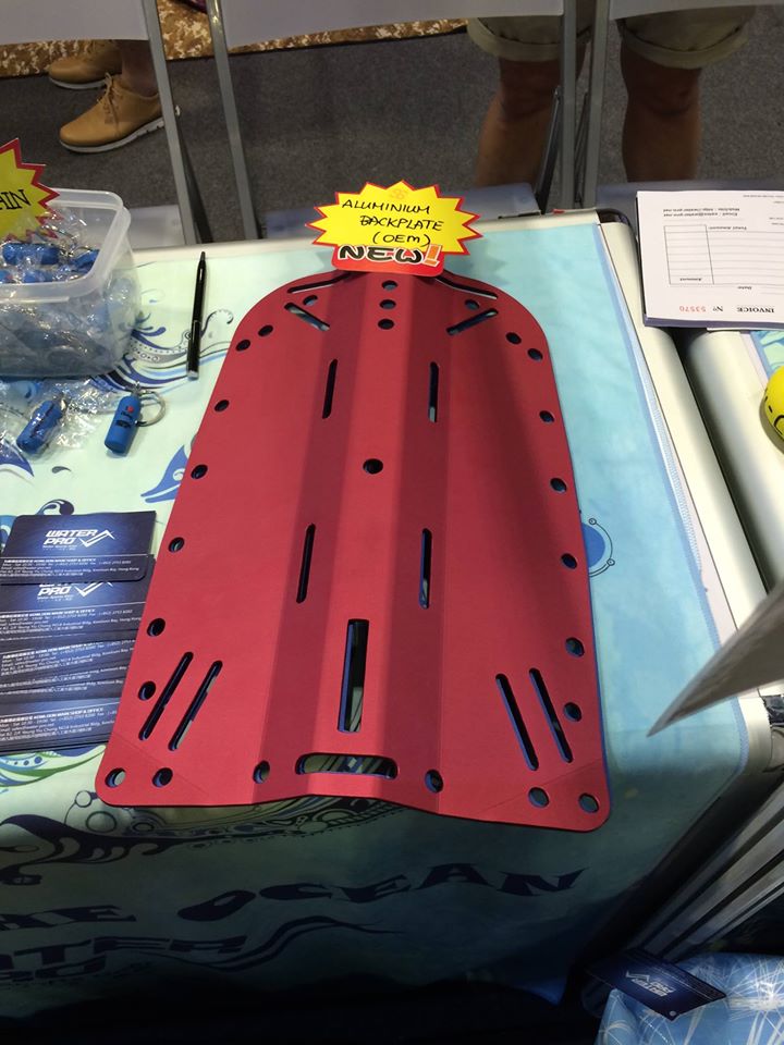
The backplate is the main question. It’s the one major component that has to fat-trimmed. I had initially thought of getting Waterpro’s anodized aluminium backplate, but thought – why not go even lighter?
Waterpro’s anodized aluminium backplate seen at ADEX 2015
Waterpro’s anodized aluminium backplate seen at ADEX 2015Whilst aluminium is lighter, it is also mechanically weaker than stainless steel, to ensure that the tough demands of technical diving loads are met; I looked into something even stronger and lighter…
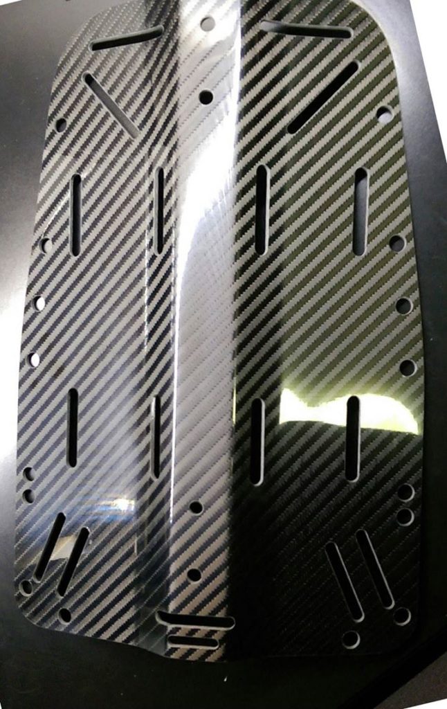
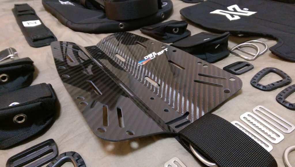
Carbon Fibre.
This is the stuff that makes Formula-1 and supercars that one can only dream of, and I was pleasantly surprised that I didn’t have to custom one as there were automobile-part manufacturers producing carbon-fibre components and body parts.
Dexcraft’s Ultra lightweight carbon fiber diving backplate weighs 400 grams with a tensile strength of 1760MPa (Mega-Pascals) and a cost $330 SGD, or €205.00, 6.75 items lighter than a steel one (2.7kg) and 2.25 times lighter than an aluminium backplate (0.9kg). The CF-backplate is made from a 4/4 unique weave. Carbon fiber reinforced polymer (CF) ensures strength a few times improved comparing to steel products of the same weight. Here’s a table of the equivalent strengths of the materials typically used to make BCD backplates:
316 stainless steel
7000-Aluminium
Carbon Fibre
Weight of backplate
2,700g
900g
400g
Tensile strength
620 MPa
295 MPa
1760 MPa
Fatigue strength (1M cycles)
303 MPa
83 MPa
1510 MPa
Strength to weight ratio
0.229
0.431
4.40
Did I mention the off the charts strength-to-weight ratio of 4.40?! That’s 19 times stronger than 316 marine-grade stainless steel. (Further information on 316-type steels, material comparison table here).
When comparing carbon fibre with other commonly used building materials. The strength and modulus (a measure of how much a material deforms under load) of carbon fibre is impressive. However it’s most important attribute is the combination of high specific strength, specific modulus and fatigue resistance. By dividing the strength and modulus values by the density, one is able to compare the weight of each material required to carry a load. A high fatigue resistance allows a structure to carry loads close to its stress limit, without the fear of unacceptably shortening its working life. Aluminium and stainless steel have poor fatigue properties.
The fatigue resistance of carbon fibre/epoxy resin composite material is far superior to both metals and other composites. It is relatively insensitive to fatigue damage even at very high stress levels. Carbon fibre, despite it’s high cost, is the ideal material, Its properties allow the BCD to be light, strong and durable. I won’t go into the specifics of metallurgy and material engineering so as not to make this entry too technical. It’s just that carbon fibre is currently the lightest and strongest material economically available that Elon musk is building his spacecraft fuel tanks with it.
I got myself a a carbon fibre backplate. It’s so pretty.
As for the bladders, the main consideration with the toughness of the outer cladding, it must be as tough as possible to resist abrasion and abuse from accidentally scraping past rocks or walls during a cave dive or against possible sharp edges in a wreck dive. Since most bladders have standard mounting rings, they will be compatible in a single-tank or twin-tank setup.
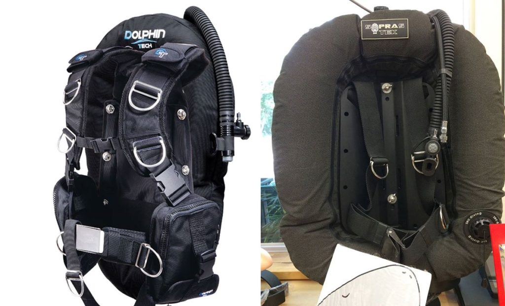
The uniformity of the donut is important for stability and balance – meaning no dead zones or air pocket traps, thus making diving trim easy and effortless. A dive trim must remain stable and with a consistently horizontal profile, regardless of the pressure in the cylinders or the amount of air in the bladder. With those considerations, the semi-finalists were a toss-up between the IST Dolphin JT-30D, Sopras Tek xTech Kevlar, Halcyon Infinity, xDeep hydros or the Scubapro x-tek donut wings. Since the weight for each of the bladders were within the ballpark of each other, the last variable consideration was cost:
Bladder
Bladder material
Approx Cost
Scubapro x-tek 30lb
CORDURA® 1680 denier
~$400
IST Dolphin JT-30D
CORDURA® 1680 denier
~$500
xDeep hydros 40lbs
CORDURA® 1100 denier
~$500
Halycon Infinity 30lbs
CORDURA® 1000 denier
~$650
Sopras Tek 40lbs
Kevlar weave
~$780
Incidentally the Sopras Tek is made from the strongest material – Kevlar, unfortunately there was scant information available from it and a concern that after-market support will be poor since it’s an uncommon brand, plus it was the most expensive of the line-up. CORDURA® Brand of Ballistic Fabric is as tough as it gets is an inter-woven yarn of nylon used to make military-grade clothing, gear and has various weave (denier) densities from 470 dTex all the way to 1680 dTex.
“Denier” refers to the weight, not the strength of an individual fibre that goes into making a fabric. Therefore, a higher denier count means a denser fabric. Strength and abrasion resistance are achieved via how the fabric is spun, or woven. These characteristics are measured through tenacity (strength per denier), breaking strength (tenacity x denier) and toughness. Cordura 1680 Denier is as tough as it gets and 1050 denier fabric meets U.S. Military Specification MIL-C-12369F-GL.
These nylon materials are sometimes known as “Rip-stop” from various manufacturers, and is used to make parachutes, gliders, tents, tarpaulins and climbing harnesses. They’re strong and don’t tear or rip easily. The Scubapro x-tek’s outer wing is made from 1680D Ballistic nylon outer shell and a 420D nylon inner bladder. I was able to get a great deal from Amazing Dive shop and ScubaPro being one of the biggest names in diving, spare parts for the inflator hose and dump valves would have been easy to procure. Scubapro X-Tek Donut Wing – 13KG Bladder (Single) bladder was thus selected.
Harness
Ok, now that the backplate and bladder is settled. I didn’t want to go around with a hard bare backplate, jumping into the water with twenty kilos of gear strapped onto it. After reviewing several backplate padding types, I decided on the xDeep 3D mesh as it was made out of a neutrally buoyant material – aramid. Aramid is a class of synthetic composites used in aerospace and military applications, for ballistic-rated body armour fabric and ballistic composites, they’re used to make fire-men’s uniforms for it’s fire-retardant properties.
Standard backplate padding’s foam material compresses at depth and might require additional weight to compensate. The softness results from springy fibres inserted in a special manner in the mesh structure. A secondary alternative I was considering was the hollis backpad combined with a 1000Denier Corduroy Molle shoulder strap, but that will just be two different manufacturers, more sources to order from, not to mention the Molle shoulder strap will take a longer time to dry.
According to xDeep – the design allows water to easily flow through the mesh, and the pressure does not have any impact on its parameters. Padding made of 3D Mesh does not compensate under pressure, is equally soft at all times and does not require additional weight. It also dries much faster than the classic foam.
Excellent, I got a set.
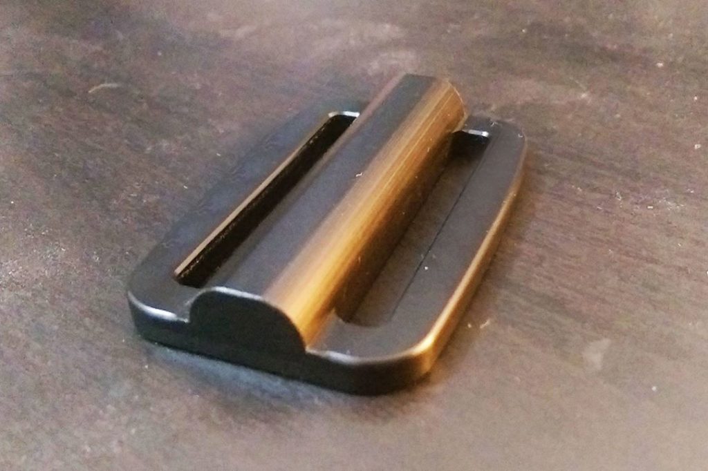
It is easier to link as many components as possible to one manufacturer/brand since shipping together reduces cost. xDeep’s webbing claimed to be made of polyamide, which is possibly simply nylon and totally resistant to water, so I got a roll and the accompanying stainless steel buckle, crotch strap, tri-glides and 316L stainless steel D-rings.
One thing I really wanted was a quick-release/adjustment system from the BCD in the event I need to release my BCD quickly to assist other divers (i.e. up a dinghy) and tested several systems. Whilst I liked the DiveRite clip system, the release buckles do present a potential weak-spot and point-of-failure. Should the plastic buckles break, overall system integrity is compromised, so the 2” webbing should retain full continuity for maximum strength.
What I found for a quick-release/adjust system was a nifty little retainer/cinch. It basically acts like a figure-8 belay device used in climbing where there is tension in one direction and reduced tension in another direction. The Cinch Quick-Adjust Harness from Halcyon specially designed for this purpose and cost S$188 in Singapore.
You can read more about the retainer in Halcyon’s patent here, the retainer accessory permits a diver to quickly adjust a one-piece continuous piece of webbing by simply pushing or pulling the webbing in the desired direction which allows the webbing to slide on through the attached accessories without affecting the location of the accessories with respect to the diver’s body.
However, I think $188 is too expensive and instead cinch adapters like this are available, or you could make it yourself. I got myself two to test and they work rather well. So now I have a continuous webbing harness that is both strong and quickly adjustable any time prior to a dive or during a dive.
Weight Pockets and carabiners
Weight belts were definitely out of the question, it’s another piece of gear to worry about when you’ve a dozen other items that could get misplaced in the hustle and bustle of diving. Many manufacturers offer “release pockets” specific to their product design and are mainly centred at the waist, the idea is that in an emergency the weight pockets can be discarded.
Well. How often does that happen? Discarding weights for an emergency ascent is a bad idea and isn’t an option at 30 metres – it simply denotes poor dive-planning, so I decided my weight pockets will just primarily be compensating in the event I have to dive in a dry-suit or 7mm wet-suit.
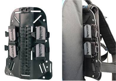
Again, I found inspiration with Halcyon’s setup where the weights are placed as close to the body as possible on the backplate itself! Great for keeping the trim horizontal and keeping weights as close to the body as possible.
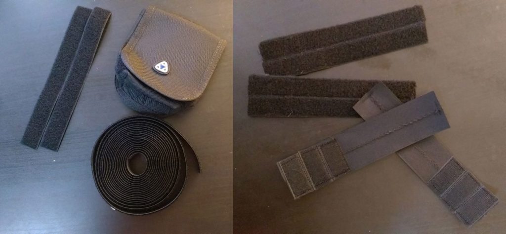
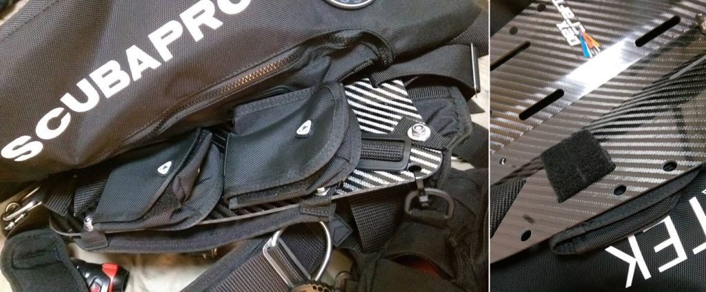
I got four affordable weight pockets from EZ-DIVE at $20+ each (although this could be another component that could be avoided for cost-savings) since it’s just a Velcro pocket. The weight pockets were designed to be slipped onto a weight belt, and to solve that, I sewed on some Velcro straps to the pockets so that it can be mounted horizontally onto my backplate.
The weights slip in from the top, and is neatly mounted onto the backplate and hidden by the bladder. Completely out of sight and unobtrusive.
Single Tank adapter and tank bands
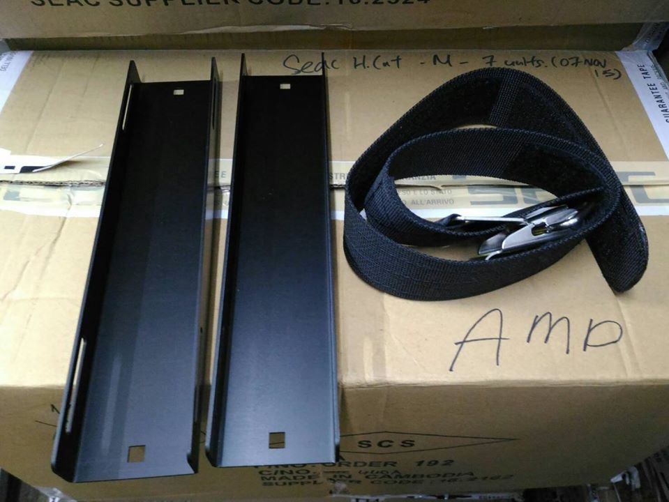
The major components are all accounted for, Carbon fibre STAs are available but cost five times more with little gain in weight savings so I got an aluminium Single Tank Adapter (STA) with 2 Super Cinch Straps for $155. The super cinch tank bands are great!
They unclasp completely so you don’t have to slide the BCD over the tank, and instead I will be able to place the BCD flat on a boat deck and place a tank on the BCD or if the tank is in a tank-rack still being charged, I will be able to mount my BCD onto the tank without having to move the tank at all. Extremely convenient over existing tank bands.
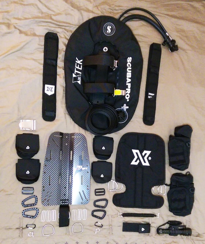
Putting it all togetherIt’s time to assemble all the components.
It’s time to assemble all the components.
As for my SMB and reel and spare mask, they are are stored in a military-style bottle holder made from 600D Nylon which actually works out very well and are mounted on the waist-webbing and attached to the backplate via cable-ties. To reduce further weight, all non-load bearing carabineers are plastic and the submersible pressure gauge (SPG) is a nice glow-in-the-dark carabineer.
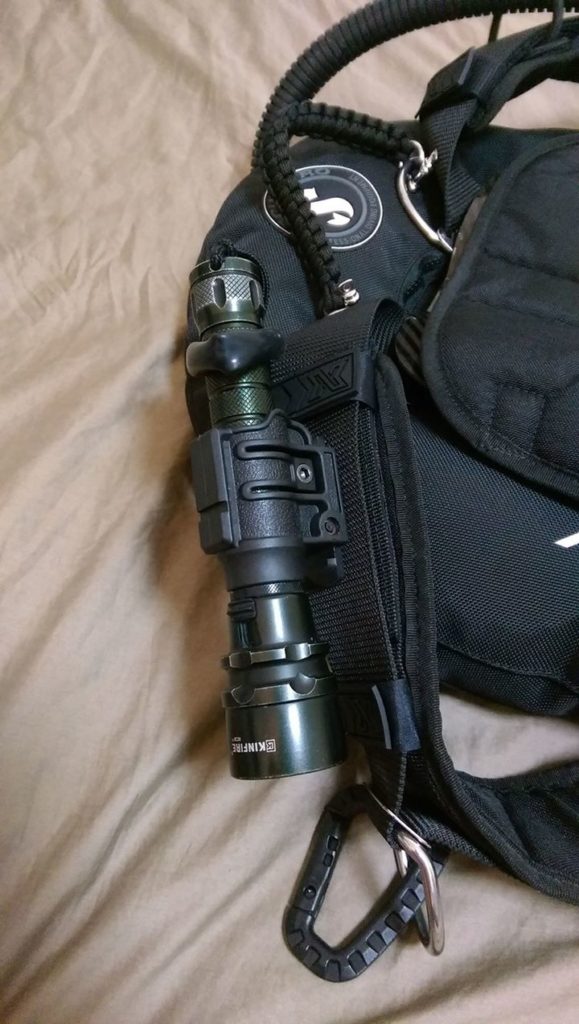
One unique feature I added is a quick-release mount for my dive-torch based on the military 26mm picatinny rail weapons mount. I decided it will be mounted on my right shoulder pad instead so that it won’t interfere with my inflator hose, and the knife will have to go to my waist webbing. With that, I now have a hands-free torch mount that I can remove and re-mount as and when I need it. It can be removed via a thumb-button with one hand.
The last feature I have is a military-grade type-III paracord, (a lightweight nylon kernmantle rope used in the suspension lines of parachutes) as handle that I’ve attached to two D-rings just aft of my bladder. This allows me to carry the BCD or hang the BCD up to dry on a hook in a more comfortable manner, plus it looks sleek and has a breaking strength of 550lbs (249kg), I won’t even be able to lift that much less worry about it breaking.
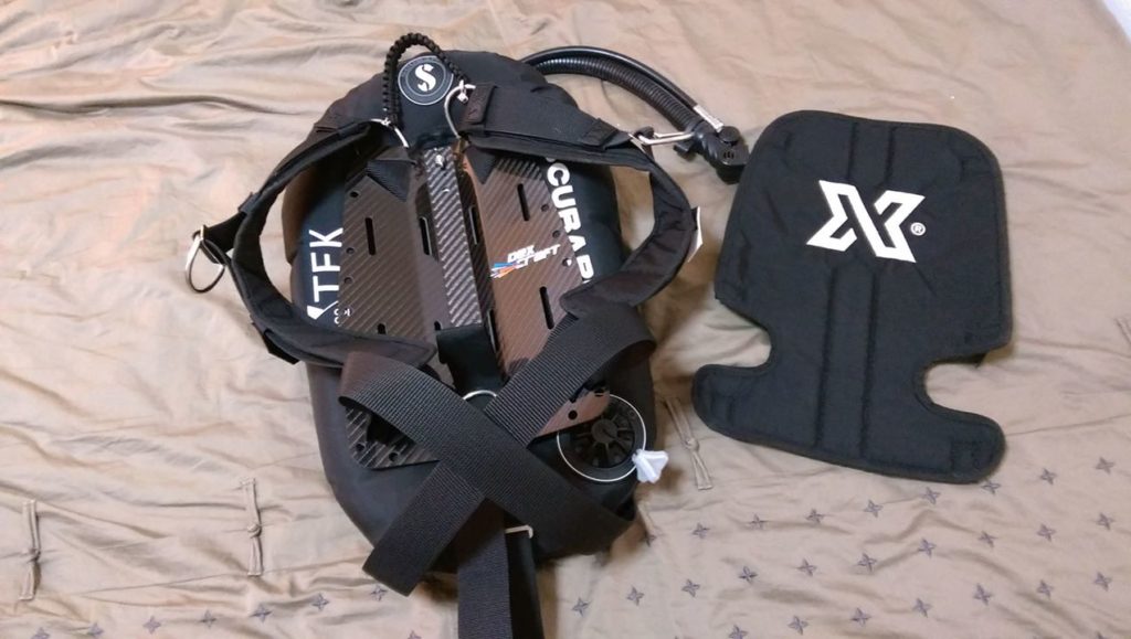
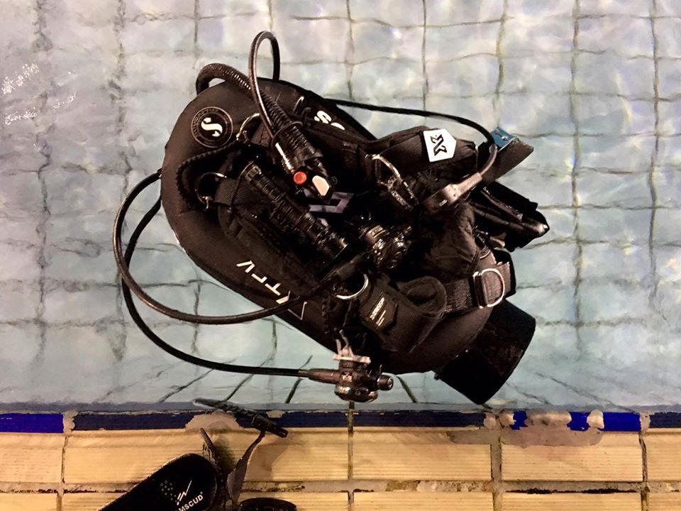
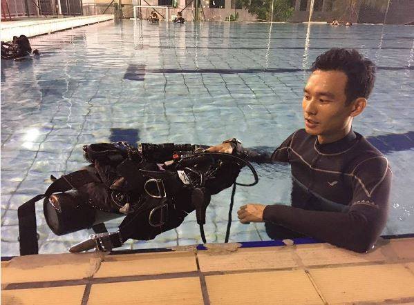
Testing and summary
I took it out to the pool for a spin, and it worked fabulously well. (I have to admit I am somewhat biased towards my own work), even in non-saline pool water, no additional weights were needed, buoyancy and trim were great, the setup felt sturdy and the ScubaPro bladder works a charm.
Field testing
The total weight of my BCD setup is a scant 2.40kg and all in all, this project cost me about S$1.2k give or-take. As of today, I’ve done about 30 dives on this BCD and so far, really satisfied with its performance. The whole endeavour of this exercise is to keep the weight low, and with all accessories mounted or in the pouches (SMB/reel/hook/knife/torch/spare/etc.), the assembly weighs 4.8kg, thus allowing further weight allowances for other gear and devices. For lighter BCDs, you’ll have other options such as travel BCDs or skeleton BCDs, unfortunately they may not provide the same flexibility or versatility as a full-fledged backplate for technical applications.
If you’re still reading this article to this point, I would like to thank you for your interest and to the various instructors, friends and fellow divers who have helped in procurement of the various components and provided me with their opinions, advice and support.
Now that the hype is all and well over the release of Apple’s iPhone 5S and iPhone 5C, with no shortage of articles written by bloggers, technocrats and aficionados all around the around the world. I’d like to add a few words to the foray and really delve into the aspects of the iPhone 5S and why I think it has what it takes to make it a win.
Well when Steve jobs departed, industry critics prophesized the demise of Apple’s innovative streak. This was true to a certain extent with market dissatisfactions over the incremental improvements of recent product releases that were lacking in ground-breaking and industry-pioneering features that Apple is well-known for.
With the recent leaks over the internet prior to the official launch of the much vaunted and eagerly awaited iPhone 5S; cyberspace has been rife with speculation and conjunctures – which so far has been accurate both in anticipated features and naming nomenclature, namely the iPhone 5C and 5S.
In this short write-up, as a techie with no affiliation to any platform, I will not re-explore debates regarding Android vs. iOS, nor will I defend any manufacturer, economy or ecosystem. I will present facts and my opinions as it is and point out the winning merits in reference of the iPhone 5S in a straightforward manner.
Aside cost, here’s a breakdown on why I think the iPhone 5S will be a phenomenal success over existing competitors and the comments on the features and components that will leave smart-phone industry giants struggling to keep up in their subsequent smartphone model releases.
Camera
There’s no doubt that the built-in camera is one of the most used feature of smartphone. Whilst the megapixel count remains the same at 8MP, Apple made significant strides in its imaging capabilities both in the hardware and software. Briefly speaking, the major advance in recent times is no longer about the megapixel race. Well-informed consumers now know that bigger megapixels doesn’t equate to better pictures. The in-speak now is pixel size, this was first discussed when Nokia released its massive 41-megapixel Pureview smartphone [1].
A major peeve in smartphone photos are noisy pictures (those grainy stuff you see when taking pictures in a dark environment). That’s because not enough light is reaching the sensor. There are two approaches to solve this problem – 1) make the pixel larger, 2) remove obstacles in front of the sensor.
Larger pixels
The larger a pixel is, the more light can be captured by the sensor. The more light captured, the better a picture will look in a darker environment. That’s why DSLR photos look good, because their sensor die areas are huge. DSLRs such as the Canon EOS 700D has an 18-megapixel APS-C sensor and 4.2μm pixel size [2], that’s four times larger than a typical smartphone camera.
As points of reference, the HTC One has a pixel size of 2.0 µm while the iPhone 5 and Nokia 808 Pureview are 1.4 µm. The HTC One was the first smartphone to feature a sensor with a larger pixel, which they called the “Ultrapixel Camera” [3], no other smartphone has yet to follow suit. Till now.
Remove obstacles
Typical CMOS sensors have transistor circuitry in front of the photodiode pixel, hence blocking some photons (light) from reaching the photodiode. To prevent that, an approach called “BSI” (Back-side illuminated) places the wiring behind the photodiode, allowing more light to reach the sensor. Without delving too deeply into camera sensor technologies, two companies who are making great BSI sensors for use in the mobile device industry are Omnivision and Sony.
Apple was using OmniVision’s OV5642 camera module inside the iPhone 4. OmniVision’s secondgeneration OV5650 and OV297AA modules were being used on the iPad 2, the new iPad and the iPod Nano. But Apple switched to Sony’s EXMOR-R sensor for the 4S and 5 [4].
Although speculation revolved around Omnivision’s 4K2K or Quad Full High Definition (QFHD) being the sensor provider for the iPhone 5S [5], iFixit revealed the camera to be Sony’s [6] with serial markings “DNL333 41GRF 4W61W”. According to Chipworks, the “DNL” serials are similar to Sony’s IMX145 sensors in the iPhone 4S and 5, and since we know that the pixel size is 1.5μm, it’s definitely a newer variant.
Whilst we don’t have exact specifications of Apple’s new iPhone 5S camera, chipworks also revealed that the sensor die is likely a Sony Exmor-RS [7]. Sony’s own Exmor-R IMX117CQT is a BSI sensor with a diagonal size of 7.81mm, 1.55 µm pixel size, 12.4 Megapixel at 35fps and can achieve 4K video (4096H x 2160V) at 60fps [8]. This is very consistent with the performance claims of the iPhone 5S.
Sony’s Exmor-R series of CMOS sensors is actually a very good choice, the larger pixels allow more light to be collected, and the Exmor-R is used in Sony’s entire line of Cybershot cameras, Blackfly’s GigE and Flea3 cameras, as well as GoPro’s HERO line of action cameras.
Leap and bounds in improvements
A plausible reason why Apple hasn’t gone into 4K video yet is probably due to memory and/or processor bandwidth limitations, but we’ll not be looking into that yet. Ok, so let’s see what the new sensor is capable of. It’s got a 15% larger sensor, 33% more light captured. A wider F2.2 aperture (compared to the F2.4 of the iPhone 4S, 5 and 5C, that means even more light) and auto image stabilization. Sapphire lens cover, 5-element lens, face-detection and photo geotagging. These are great, but they already exist in consumer point-and-shoots, so what really takes the cake?
For starters, the Slow-Motion (Slo-Mo) feature was first featured in Casio’s High-speed EXLIM line of point-and-shoot cameras in 2010 [9], that feature brought about stunning footage, but wasn’t compelling enough to buy over enough consumers. Then action camera company GoPro released their line of HERO action cameras [10] and a mass marketing campaign that birthed an industry of action cameras [11].
The GoPro HERO line of cameras was a remarkable success, which featured incredible high resolution slo-mo footage. Here’s the kicker. ow the iPhone 5S can do the same. The iPhone 5S can shoot 720p at 120fps footage, this capability bests GoPro’s Hero3 Silver or white edition and can match the GoPro’s flagship black Edition at the lowest setting 720p, the real kicker is that the GoPro retails at $329.99, but for US$399, you can get the 64Gb version of the iPhone 5S!
Between US$329.99 and US$399, what would be the likely choice of consumers? Let’s explore the situation – I would likely carry my phone everywhere I go, but not my action cam. What’s to stop me from getting a water-proof casing and turning my iPhone into an action cam? Waterproof protective casings are widely available [12, 13].
Moreover, with my iPhone 5S, I can take pictures, view and edit and share my footage all on one device instantaneously. Something the GoPro Hero3 has limitations with. There’s no attached LCD screen (unless you buy an attachment), the battery life is a dismal 2.5 hours per charge. Even with the Wi-Fi attachment to a GoPro, I’ll still need my smartphone with Wi-Fi-enabled iOS app to control the GoPro camera.
To further add to the injury, the iPhone 5S is capable of continuous burst mode 10fps photo-stitching mode, 1080p HD video at 30fps, it has live video zoom with auto image stabilization, multiple photos shooting mode. The Slo-Mo video and regular video can be combined to create all new video effects. In Panorama mode, the iPhone 5s can capture 30 fps, which is a 50% improvement over the iPhone
5, plus auto white-balance, exposure, dynamic tone mapping, a 15-point autofocus metering [14].
Continuous 10fps burst mode and 15-point metering? That’s seriously DSLR stuff! Besides, most DSLRs can’t do 120fps, most topping out at 60fps. As an owner of a DSLR system myself, I find that due to the sheer convenience of my smartphone camera, I often avoid the hassle of taking my DSLR out of its dry box.
The iPhone 5S could possibly the single most devastating competitor to the action camera industry, the consumer point-and-shoot camera industry and the prosumer camera market. The features of the iPhone 5S overlap whole product portfolios in both action cam market segments and DSLR markets. With the iPhone 5S, anyone can be a super-photographer/videographer now.
Camera Flash
As a photographer myself, what can we say about this feature of the iPhone 5S? It’s an incredible innovation that is a world’s first! Apple’s solution to a common flash whiteout is so deceivingly simple and yet so effective it has gotten me thinking, “why hasn’t anyone thought of that before?”
Anyone who has used a flash before would have noticed a “white-washout” of faces, that’s because the harsh glare of the LED/xenon flash is not the same colour temperature as human skin, which is of a warmer 3000 Kelvins. Redder colours are “warmer” and have a colour temperature closer to 1000K, whilst bluish-whiter lighting has a colour temperature closer to 10,000K.
To solve the problem of a flash white-out on people’s faces, Apple’s solution is the “true-Tone flash”
and it is truly an original marvel for casual and avid photographers alike [15]. Simply put, two LEDs of different colour temperatures (cooler white and warm amber) is used to create a colour variance to match the ambient colour temperature of the environment where the photo is being taken.
This feature is not just a world’s first on any smartphone; it’s also the world’s first on any camera! Have I already mentioned that the camera has capabilities comparable to point-and-shoots and DSLRs?
Industry-Leading A7 64-bit Processor
As always in the smartphone wars, performances of new devices are always compared with existing market flagships such as the Samsung Galaxy S4 [16] and the HTC One [17], sporting a powerful Qualcomm Snapdragon 600 processor that even the Apple iPhone 5 had trouble competing with.
But the custom 64-bit A7 in the iPhone 5S has a performance improvement almost an order of magnitude better over its predecessors, with phenomenal performance comparable to that of Intel’s latest quad-core Bay Trail processors (it is also impressive that the A7 has only got 2 cores!) [18].
Even Sony’s latest flagship phone, the Xperia Z1 will utilizing Qualcomm’s top snapdragon 800 processor, is still a 32-bit 2.3 GHz Quad-core CPU has a slower 12.8Gb/s memory speed. Moreover, independent tests have consistently shown the iPhone to be more responsive than any of its Android counterparts [19, 20].
Processor Comparisons
Phone
iPhone 5S
iPhone 5, 5C
Galaxy S4
HTC One
Advantage?
Processor
A7
(APLX069)
A6
(APL0598)
Exynos 5 Octa
-5410
Qualcomm
Die
Area
102 mm2
96.71 mm2
122 mm2
88.09 mm2
Smaller is better
Process
28nm
32nm HKMG
28nm HKMG
28nm LP
Smaller is better
Clock
speed
1.7Ghz
1.3Ghz
1.6Ghz
1.7Ghz
Higher is better
Cores
2
2
4x Cortex-A15
4x Cortex-A7
4
Address
64-bit
32-bit
32-bit
32-bit
IPhone 5S
Instruction
set
ARMv8
ARMv7
ARMv7
ARMv7
IPhone 5S
Memory
1Gb
1Gb
2Gb
2Gb
Galaxy S4/HTC
Memory
channels
4
2
2
2
IPhone 5S
Memory
type
LPDDR3-1333
LPDDR2-1066
LPDDR3
LPDDR2-1066
IPhone 5S
Memory
freqeuncy
533 Mhz
533 Mhz
800 Mhz
533 Mhz
Galaxy S4
Memory
speed
17Gb/s
8.528Gb/sec
12.8Gb/s
8.53Gb/sec
IPhone 5S
Hype over 64-bit
Without delving too deeply into the technical details, having the first 64-bit processor in a mobile device is a major win point for the iPhone 5S. The A7 is the world’s first 64-bit mobile processor, but what does that mean?
Simply put, chips with more bits can handle more memory. A 32-bit chip is designed to handle memory addresses of up to 32-bits while a 64-bit chip is designed to handle memory addresses of up to 64-bits. The advantages of 64-bit are that more RAM can be addressed; the push to 64-bit architectures will be fully appreciated in high-performance server clusters where more memory is actually needed.
ARM first announced the new 64-bit architecture in October 2012 [21], which described the CortexA57 and Cortex-A53 processors eaturing multi-GHz performance on advanced FinFET processes technologies. Back then, only a few large players in the semiconductor industry announced that they will be entering the mobile 64-bit platform using the ARM architecture [22]. Even then production was only slated to begin in 2014 [23], and from then it will take some time before it trickles into the hands of consumers.
One thing is for certain, no one saw it coming. Even veterans in the industry were surprised during the keynote announcement of the 64-bit architecture in the A7. The A7 was made available to the public barely 11 months after the original announcement made by ARM, which is commendable on how fast Apple managed to design and manufacture the chip completely under the radars of global chip-giants.
Apple isn’t the only company building their own SoCs (System on Chip) processors, the ARM architecture is being modified by chipmakers all around the world. Semiconductor giant Samsung has their latest Exynos, Qualcomm’s snapdragon series, NVidia’s Tegra series, Texa’s Instruments OMAPs, Freescale’s i.MX and so on and so forth.
What’s remarkable is that Apple isn’t in the business of selling chips. They built the A7 because no other chip was good enough! On paper the A7 is already superior to NVidia’s next-generation Tegra 5 “Logan”, which will be running a Quad-core cortex-A15 ARMv7 28nm process that is not available in any consumer device yet and will only be released in Q2 2014. Furthermore, the A7 can already be said to match NVidia’s touted claims of its Tegra 6 “Parker”, which will be running NVidia’s 64-bit solution, is slated to be released in 2015. Based on these projected timelines, the iPhone 5S is industry leading by at least one to two entire years.
This diminutive chip has shaken up semiconductor giants in the mobile processor industry. The desktop PC industry took over 10 years to transit from 32-bit to the common 64-bit we have in our computers today, hence it is a logical move for Apple to have introduced the 64-bit architecture in the A7. It’s arguable that 64-bit doesn’t boost performance for a mobile device for now [24], but as with the progression of hardware, eventually smartphones will arrive with 4Gb of RAM. When that happens, Apple will not only have the hardware but an entire application and operating ecosystem that can take advantage of the full benefits of 64-bit [25].
Hardware and Software Integration
Given that the industry momentum will take time to make the transition to 64-bit, Apple’s 64-bit chip will already have laid the foundation for the software market to catch up. How did Apple managed to win the mobile wars so suddenly and so decisively?
The tight integration of software and ecosystem has allowed Apple to release new products without being tied down by external supplier constraints. The biggest point we must look here is that Apple now already has a commercially available 64-bit processor in its newest flagship smartphone, and in terms of software, the 64-bit iOS that was developed in-house would have immediate and unrestricted access to the architecture of the hardware.
However, integration and cooperation between development of Android OS and hardware application processors are not as tightly integrated as the iOS ecosystem and Android OS users have traditionally suffered from OS fragmentation. Android devices obsolete quickly where new OS releases are not compatible with older hardware and users are left without future updates [26-31], a situation made worse when developers release apps for iOS earlier than for the Android platform [32], this is also a reason why iTunes has been a tremendous commercial success, consumers on the iOS can buy creative content on the go, but Android users are left lacking [33]. The ball will keep rolling; developers will now be driven to transit to the iOS platform, where a 64-bit architecture is already ready.
Little is known about Google’s upcoming Android OS, Kit-Kat 4.4 [34], but for hardware manufacturers the cat and mouse game begins. If the OS isn’t 64-bit yet, so why build a 64-bit processor? Even if Samsung releases a 64-bit processor, the OS won’t support it [35], or if Google releases a 64-bit OS, none of the existing applications processors can run it. It’s the chicken and the egg story again.
The A7 64-bit processor of the iPhone 5S isn’t a selling point for one smartphone; rather, it’s a long-term future-proof selling point for the entire iOS app ecosystem.
Becoming an independent chipmaker
Unlike most other phone vendors, Apple began designing its own custom processors after the release of iPhone and has been incrementally acquiring chip-design firms such as PA Semi [36], Anobit [37], Intrinsity [38] and AuthenTec [39] and aggressively building its own chip design team [40, 41].
These acquisitions have helped Apple build a series of increasingly customized SoCs called the “Aseries”. The first few generations of processors were originally manufactured by Samsung [42] and is also confirmed as the manufacturer of the A7 [7].
With several years of chip-design experience since the introduction of their first in-house designed processor, the A4, Apple has made considerable advances in chip-design know-how [43, 44] and is now actively seeking manufacturing capabilities.
Building a fabrication plant is extremely expensive and there aren’t many semiconductor fabrication plants in the world that can manufacture chips on such a scale. Most semiconductor firms are fabless (e.g. Qualcomm, NVidia, Broadcom, AMD, Marvell and Xilinx etc.). A company that operates a fabrication plant for the purpose of manufacturing the designs of other companies and do not produce ICs of their own design are known as “Pure-Play” foundries, some of world’s biggest pure-play foundries based on revenue are TSMC, UMC, Global foundries and SMIC [45].
Semiconductor industry mega-giants who can fab their own chips are known as “Integrated Device Manufacturers” or IDMs. Intel, Samsung, NXP, STMicro, Freescale, Cypress, National Semiconductor, Texas Instruments, Infineon, Bosch and a few other smaller players.
One question begs to be answered, why did Samsung use its competitor Qualcomm Snapdragon 600 processors in a variant model of its flagship Galaxy S4 and Note 3 instead of its own Exynos 5 processor? Of the amount of resources spent in developing the octa-core Exynos 5, the high cost and performance could have forced Samsung to use a competing chip in its devices. Signs show that Samsung is losing the race [46] and manufacturing contracts from Apple [47-49].
Apple now has both Samsung, TSMC and Global UniChip to manufacture its chips [50, 51], but TSMC and Global Foundries both make the competing Snapdragon processor for Qualcomm, which is used to power the HTC One and Galaxy S4 smartphones, so much less is needed to be said about Samsung being the primary contractor for Apple’s A7 chips.
There is evidence that Apple building its own fabrication capability to reduce reliance of competing foundries [52, 53], and this is true, Apple will be moving into a new strategic direction to create its own chips, completely making itself independent of rival foundry manufacturing facilities and further shrouding itself in technological secrecy, most important of which Apple will no longer need to share IP about its new products with Samsung or any other rival firm for that matter.
With its market capitalization, cash in the bank and development in this direction, Apple will become a force to be contended with in the semiconductor industry.
M7 Motion Co-processor
There’s nothing new here, basically an integrated accelerometer, gyroscope and a compass. The Galaxy S4 is using Invensense’s MPU-6050 and the HTC’s One is using the Invensense MPU-3050 which has similar capabilities. But what’s the industry-shaking news regarding this diminutive little chip that most of us take for granted in our own smartphones?
The thing is, the M7 doesn’t need the A7 to work. It’s an independent SoC, with the M7 constantly monitoring movement, this feature overlaps wellness devices like the Fitbit and jawbone [54]. Given the rich iOS ecosystem, built-in radio communication and various other advantages that a smartphone will have that discrete tracking health devices doesn’t have, fitness gadget manufacturers are going to see a major chip in their sales when consumers choose a smartphone that can already do what a wellness tracker can do and more [55].
Whilst existing wellness devices tout other features, the iPhone 5S is a fearsome contender in the growing wearable’s market that other wellness companies are paying attention to right now [56, 57]. Fitness giant Nike has taken the lead by integrating Nike+ move app for use with the M7 [58].
Chipworks provided a lot of insight into the M7 system [7]. It turns out that the M7 is not an integrated 9-DOF (degree of freedom) MEMs sensor. It’s simply a discrete ARM Cortex-M3 microcontroller based on the LPC18A1 by NXP, the LPC1800 series is 120Mhz 32-bit MCU [59].
It is a separate MCU processing data from the 3 discrete MEMs sensors – Bosche Sensortech BMA220 3-axis accelerometer [60], ST microelectronics gyroscope and Asahi Kasei Microdevices’s AK8963 3-axis compass [61]. Why Apple didn’t choose to use other established industry MEMs sensors like STmicro, Freescale or Invensense can only be speculated. We also need to note that Invensense has repeatedly lost out to other MEMs providers in Apple’s decision-making process.
The advantages of having the M7 is tremendous, battery consumption is reduced during tracking as the A7 isn’t engaged. Your phone will now know when you parked your car and maps could transit from diving mode to walking [62, 63]. If you’re moving the phone won’t ask you to join a Wi-Fi network and if you’re sleeping, network activity will decrease to future extend battery life [64, 65].
The M7 system is like a little Fitbit or jawbone within the iPhone 5S, when this feature was first announced, analysts were surprised too, it’s a new direction for apple although several clues have shown Apple’s desire to enter the wearable electronics market [66, 67], and it could serve as an ominous tracking device, reducing our nearly non-existent privacy further [57].
TouchID Fingerprint Sensor
A much-vaunted feature of the iPhone 5S worth shining the spotlight on is the Touch ID biometric sensor. Fingerprint sensors have been around for some time and are present in many PDAs (who uses that term anymore) and business laptops, but if it’s so secure, why hasn’t it been widely adopted by the mobile industry?
Well, the capacitive swipe-down type of fingerprint sensor hasn’t been exactly easy to use and too often reads erroneously, creating consumer frustration. Optical fingerprint sensors used at security checkpoints are far too bulky to be installed in a mobile device. There are many OEM fingerprint providers in the market, with big names such as Motion Micro Solutions [68], DigitalPersona [69], Fingerprints [70], Validity [71], so why did Apple choose not to adopt existing sensors but instead develop their own?
Getting it done right
The tricky balance of biometric security and ease of use has always been at the expense of each other. Most sensors don’t do a very good job at reading fingerprints, are too bulky or utilize too much power for a mobile device, but Apple’s TouchID seems to have all those issues covered [72, 73] with hardware encryption and security integrated at a native level within the processor architecture [74], something unseen is existing fingerprint scanners.
Apple has taken a very thorough and methodical approach with the release of Touch ID system and we can see that there has been a fantastic amount of convergence work done. Efforts spanned several years and have included many patent applications, acquisitions, a custom processor and the integration of ARM’s TrustZone suite all unified together into what we know now as the Touch ID.
No competition
Its clear Apple bought AuthenTec specifically for its fingerprint sensors. After closing the deal, Apple sold off the company’s encryption technology [75]. It is not only the first and only fingerprint sensor in a smartphone today; the sensor is no ordinary swipe-down type capacitive either. To tighten things further, Apple’s AuthenTec TouchID technology will remain exclusively to Apple, the technology will not be released to developers [76] and competitors will not be able to purchase it [77, 78].
With the proprietary TouchID sensor, the iPhone 5S possibly being the most secure smartphone ever [74, 79], the iPhone 5S could be the single device creating a sudden massive consumer demand boom in online commerce transactions. If it works as advertised, this will likely be the best combination we’ve seen of smartphone security and convenience.
This mobile device is going to generate millions of dollars in online revenue in consumer dollars [80], and although not demonstrated yet, in the near future through retail payment card transactions [74, 81], which is major motivational factor for retailers and merchants to scramble to accommodate and accept iOS transactions, a major self-generating cycle of win for Apple.
Battery Life
Battery Comparisons
Device
iPhone
5
iPhone
5S
iPhone
5C
Battery
Size (Whr)
5.45
5.92
5.73
Battery
Size (mAh)
1440 mAh
1570 mAh
1507 mAh
Well it only makes sense to add a bigger battery and shrink the electronics if the overall volume must remain the same, Apple advertises a modest 10 hours of talk time, LTE or Wifi internet browsing, 250 hours of standby time. Anandtech managed to dig out some details from FCC [82], and this has been confirmed from teardowns [6, 83].
It is now revealed that the battery is made by Desay Batter Co., Ltd from Huizhou, China [84]. Whilst retaining the similar form factor and build volume over its predecessors, the 5S has managed to retain its talk time to 10 hours (equal with the iPhone 5 and 5C) and standby time to 250 hours as compared with the older iPhone 4S with 8 and 200 hours respectively. This bests the S4’s 7-hour talk time.
That’s two full days of standby time (granted most of us are already accustomed to charging our phones daily). We also must keep in mind that the hardware being utilized is far more advanced, (64-bit M7, TouchID sensor, M7 processor), so it’s a notable improvement.
Conclusion
Amongst the various consumers that I had the opportunity of discussing the volition of their choice of smartphones, I learnt that what type of technology doesn’t really matter. As long as it’s got a great battery life, looks good, works well and takes great pictures. Despite industry criticisms, the “smaller” screen size of the iPhone hasn’t deterred consumers and sales have been booming [85].
With new acquisitions in semiconductor expertise, mapping, security, an entire slew of innovative features in the iOS7 environment, the features and strategic decisions that Apple has made so far will be entirely in their favour. Comparisons have already been made between the existing flagship competitors [86-89], but the iPhone 5S already has a series of distinct features – particularly its leading ecosystem and a lock on important content and enterprise markets, further increasing its lead by standing out in an otherwise poorly differentiated market of smartphones.
In summary, Apple has over-delivered expectations with new and unexpected capabilities. The iPhone 5S has challenged industry giants across markets and is going to shake up entire industries. I might not be wrong to speculate that executives at dozens of companies now are biting their nails and holding emergency meetings to discuss on what the impact of the iPhone 5S will do to their portfolios.
Industry analysts are already predicting massive successes of the new iPhone 5S [90], and the launch weekend saw a record number of 9 million new iPhones sold [91, 92]! Trends are already pointing towards favorable consumer responses in converting consumers over to its iOS ecosystem with the new iOS7 [93].
With all the factors in the equation, I believe the iPhone 5S is going to be a massive success for Apple in the months to come.
Sony, IMX117CQT Diagonal 7.81 mm (Type 1/2.3) Approx. 12.40M-Effective Pixel HighSpeed, High-Sensitivity Back-Illuminated Color CMOS Image Sensor for Consumer Digital Still Cameras and Camcorders. 2012.
Staff, A. Apple buys chip designer PA Semi for $278 million. 2008 Wednesday, April 23, 2008, 05:00 am PT (08:00 am ET) [cited 2013 18th September 2013]: http://appleinsider.com/articles/08/04/23/apple_buys_chip_designer_pa_semi_for_278_millio n.html